-
How to Use a Fully Differential Amplifier as a Level Shifter
How to Use a Fully Differential Amplifier as a Level Shifter
Loren Siebert
Many signal paths are direct current (DC)-coupled, and this can lead to challenges when different portions of the signal path require different operating conditions. Many portions of a signal path are ground-referenced, where a signal varies at about an average or mid value of 0V. If all signals had the same reference voltage, DC coupling would be very easy. Unfortunately, that is not the case. Devices operating from a single supply like mixers or analog-to-digital converters (ADCs) will typically have a reference voltage (common mode) that is not 0V. Interfacing these devices while preserving DC information can be challenging.
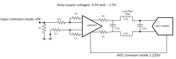
Some circuit components such as fully differential amplifiers (FDAs) can help with this challenge. Making the best use of the FDA common mode shift capability requires some advanced planning, however. The first design consideration is to map out all of the DC operating points of your circuit in order to find which voltages need shifting and in what direction. The next step is to choose a power-supply configuration that will ease the voltage shift. While many devices operate from a “single supply,” it may not be possible to have all of your supply voltages positive. Figure 1 shows a simple example.
 Figure 1 Typical Common-mode Shift
Circuit
Figure 1 Typical Common-mode Shift
CircuitAs Figure 1 shows, the signal of interest is ground-referenced while the ADC input must be centered on 1.225V. The LMH5401 is a very broadband, DC-coupled FDA that can provide a common-mode shift. The LMH5401 can operate with about 0.5V of offset on the output and 1.0V on the input. The system shown in Figure 1 requires 1.225V of shift. By combining input and output shifts, you can achieve the necessary shift in one stage. The circuit does require custom power supplies of +3.5V and -1.5V. Simple, inexpensive switching power supplies can provide these supply voltages from a single 5V board supply bus.
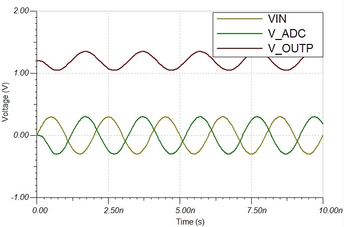
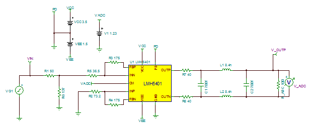
The graph in Figure 2 shows the results from the circuit in Figure 3. Because differential probes will not capture common-mode data, you will need at least one single-ended probe in your circuit to measure the common-mode voltage. In Figure 3 there is only one such probe: V_OUTP. Because there is no DC offset shown in V_ADC (the differential probe), you know that the amplifier output pins are symmetrical and you don’t need another probe. The input signal is both single-ended and ground-referenced, so only one probe is required to capture the input signal.
 Figure 2 Voltage Levels
 Figure 3 TINA-TI™ Schematic
DC voltage levels can be very challenging in a system design. By taking advantage of flexible power-supply voltages and amplifiers like an FDA, you can DC-couple signals that have different average (common-mode) voltages.
What is your experience with FDAs? Log in and leave a comment.
Additional Resources
- Download the TI Designs reference design, Two Stage Cascaded 8GHz Amplifier Reference Design Board (TIDA-00659).
- Read the application note, “Common Design Challenges and Proper Use of Fully Differential Amplifiers (FDA)” to learn about FDAs.
- Read more fully differential amplifier blogs.
- Learn about TI’s entire portfolio of amplifier ICs and find technical resources.
IMPORTANT NOTICE AND DISCLAIMER
TI PROVIDES TECHNICAL AND RELIABILITY DATA (INCLUDING DATASHEETS), DESIGN RESOURCES (INCLUDING REFERENCE DESIGNS), APPLICATION OR OTHER DESIGN ADVICE, WEB TOOLS, SAFETY INFORMATION, AND OTHER RESOURCES “AS IS” AND WITH ALL FAULTS, AND DISCLAIMS ALL WARRANTIES, EXPRESS AND IMPLIED, INCLUDING WITHOUT LIMITATION ANY IMPLIED WARRANTIES OF MERCHANTABILITY, FITNESS FOR A PARTICULAR PURPOSE OR NON-INFRINGEMENT OF THIRD PARTY INTELLECTUAL PROPERTY RIGHTS.
These resources are intended for skilled developers designing with TI products. You are solely responsible for (1) selecting the appropriate TI products for your application, (2) designing, validating and testing your application, and (3) ensuring your application meets applicable standards, and any other safety, security, or other requirements. These resources are subject to change without notice. TI grants you permission to use these resources only for development of an application that uses the TI products described in the resource. Other reproduction and display of these resources is prohibited. No license is granted to any other TI intellectual property right or to any third party intellectual property right. TI disclaims responsibility for, and you will fully indemnify TI and its representatives against, any claims, damages, costs, losses, and liabilities arising out of your use of these resources.
TI’s products are provided subject to TI’s Terms of Sale (www.ti.com/legal/termsofsale.html) or other applicable terms available either on ti.com or provided in conjunction with such TI products. TI’s provision of these resources does not expand or otherwise alter TI’s applicable warranties or warranty disclaimers for TI products.
Mailing Address: Texas Instruments, Post Office Box 655303, Dallas, Texas 75265
Copyright © 2023, Texas Instruments Incorporated