Reduce Inrush Current Using Load Switches
In most systems, capacitors are placed throughout a design to ensure there are no supply-rail voltage drops. When power is initially applied to the system, charging these capacitors can result in an inrush current that can cause several problems for the system if unaddressed.
Figure 1 shows an example system that uses a power supply – DC/DC, low dropout (LDO) regulator, or external supply – to supply voltage to a downstream load.
 Figure 1 Typical Power
Distribution
Figure 1 Typical Power
DistributionUpon system startup, the power supply will ramp up to the regulated voltage. As the voltage increases, an inrush of current flows into the uncharged capacitors. This inrush current can also be generated when a capacitive load is switched onto a power rail and must be charged to that voltage level. The amount of inrush current into the capacitors is determined by the slope of the voltage ramp, expressed as Equation 1:
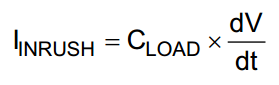
Where IINRUSH is the amount of inrush current caused by a capacitance, C is the total capacitance, dV is the change in voltage during ramp up and dt is the rise time during voltage ramp up.
Challenges with Inrush Current
There are two key design challenges associated with inrush current. The first challenge is exceeding the absolute maximum current ratings of the traces and components on the circuit board. All connectors and terminal blocks have a specific current rating that could cause damage to these parts if exceeded. Likewise, all PCB traces are designed with a certain current-carrying capability in mind and are also at risk for damage.
But appropriately designing for a large inrush current peak will lead to thicker PCB traces and more durable connectors, which can increase the size and cost of the overall design. With reduced inrush current, you can optimize these traces and connectors for a smaller, less expensive design.
The second challenge occurs when a capacitive load switches onto an already stable voltage rail. If the power supply cannot handle the amount of inrush current needed to charge that capacitor, then the voltage on that rail will be pulled down. Figure 2 shows this behavior.
 Figure 2 Power-Supply Dip Due to Inrush
Current
Figure 2 Power-Supply Dip Due to Inrush
CurrentHow to Design for Inrush Current: TPS22975 Application
You can reduce inrush current by increasing the voltage rise time on the load capacitance and slowing down the rate at which the capacitors charge. All TI load switches feature a controlled output slew rate to mitigate inrush current. Figure 3 shows the typical application circuit for a load switch.
 Figure 3 Typical Load Switch Application Circuit
Figure 4 shows a 5-V power supply brought down to 1.8 V using a buck converter. After the 1.8-V rail powers up, a 100-µF capacitance is applied to the system.
 Figure 4 System Block Diagram without
Slew-Rate Control
Figure 4 System Block Diagram without
Slew-Rate ControlWith no controlled rise time, the switch does not provide any inrush current management; see the results in Figure 5.
 Figure 5 Inrush Current and Voltage
Drop without Slew-Rate Control
Figure 5 Inrush Current and Voltage
Drop without Slew-Rate ControlFigure 6 shows the same system, except the TPS22975 load switch (with controlled rise time) switches the capacitive load.
 Figure 6 Inrush Current and Voltage
Drop with Slew-Rate Control Using the TPS22975
Figure 6 Inrush Current and Voltage
Drop with Slew-Rate Control Using the TPS22975The controlled rise time prevents the voltage drop in the supply voltage and reduces the inrush current to a manageable amount.
Large capacitance can lead to inrush current, resulting in device damage, system instability or undesired behavior. Using a TI load switch is both a size- and cost-efficient solution for managing inrush current.
Additional Resources
- Download the following application notes:
IMPORTANT NOTICE AND DISCLAIMER
TI PROVIDES TECHNICAL AND RELIABILITY DATA (INCLUDING DATASHEETS), DESIGN RESOURCES (INCLUDING REFERENCE DESIGNS), APPLICATION OR OTHER DESIGN ADVICE, WEB TOOLS, SAFETY INFORMATION, AND OTHER RESOURCES “AS IS” AND WITH ALL FAULTS, AND DISCLAIMS ALL WARRANTIES, EXPRESS AND IMPLIED, INCLUDING WITHOUT LIMITATION ANY IMPLIED WARRANTIES OF MERCHANTABILITY, FITNESS FOR A PARTICULAR PURPOSE OR NON-INFRINGEMENT OF THIRD PARTY INTELLECTUAL PROPERTY RIGHTS.
These resources are intended for skilled developers designing with TI products. You are solely responsible for (1) selecting the appropriate TI products for your application, (2) designing, validating and testing your application, and (3) ensuring your application meets applicable standards, and any other safety, security, or other requirements. These resources are subject to change without notice. TI grants you permission to use these resources only for development of an application that uses the TI products described in the resource. Other reproduction and display of these resources is prohibited. No license is granted to any other TI intellectual property right or to any third party intellectual property right. TI disclaims responsibility for, and you will fully indemnify TI and its representatives against, any claims, damages, costs, losses, and liabilities arising out of your use of these resources.
TI’s products are provided subject to TI’s Terms of Sale (www.ti.com/legal/termsofsale.html) or other applicable terms available either on ti.com or provided in conjunction with such TI products. TI’s provision of these resources does not expand or otherwise alter TI’s applicable warranties or warranty disclaimers for TI products.
Mailing Address: Texas Instruments, Post Office Box 655303, Dallas, Texas 75265
Copyright © 2023, Texas Instruments Incorporated