SLVS569F January 2005 – August 2015 LM2575
PRODUCTION DATA.
- 1 Features
- 2 Applications
- 3 Description
- 4 Revision History
- 5 Pin Configuration and Functions
- 6 Specifications
- 7 Detailed Description
-
8 Application and Implementation
- 8.1 Application Information
- 8.2
Typical Application
- 8.2.1 Design Requirements
- 8.2.2
Detailed Design Procedure
- 8.2.2.1 Input Capacitor (CIN)
- 8.2.2.2 Output Capacitor (COUT)
- 8.2.2.3 Catch Diode
- 8.2.2.4 Inductor
- 8.2.2.5 Output Voltage Ripple and Transients
- 8.2.2.6 Feedback Connection
- 8.2.2.7 ON/OFF Input
- 8.2.2.8 Grounding
- 8.2.2.9 Reverse Current Considerations
- 8.2.2.10 Buck Regulator Design Procedure
- 8.2.2.11 Inductor Selection Guide
- 8.2.3 Application Curves
- 9 Power Supply Recommendations
- 10Layout
- 11Device and Documentation Support
- 12Mechanical, Packaging, and Orderable Information
1 Features
- Adjustable With a Range of 1.23 V to 37 V and ±4% Regulation (Max) Over Line, Load, and Temperature Conditions
- Specified 1-A Output Current
- Wide Input Voltage Range 4.75 V to 40 V
- Uses Readily Available Standard Inductors
- 52-kHz (Typical) Fixed-Frequency Internal Oscillator
- TTL Shutdown Capability With 50-μA (Typical) Standby Current
- High Efficiency…as High as 88% (Typical)
- Thermal Shutdown and Current-Limit Protection With Cycle-by-Cycle Current Limiting
- For the Full Offering of Voltages (Including Fixed-Output Options) and Packages (Including TO-263), See TL2575 Data Sheet, SLVS638
2 Applications
- Simple High-Efficiency Step-Down (Buck) Regulator
- Pre-Regulator for Linear Regulators
- On-Card Switching Regulators
- Positive-to-Negative Converter (Buck-Boost)
3 Description
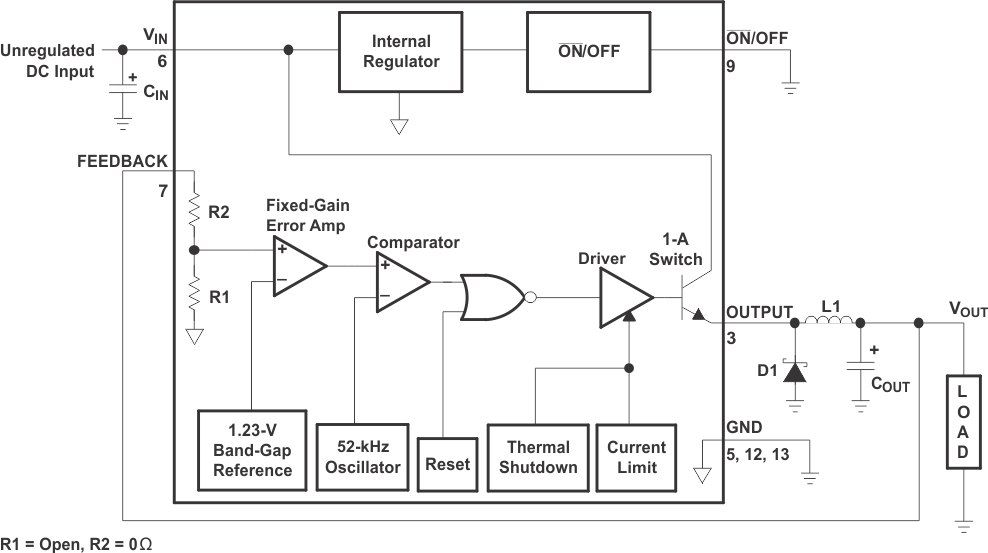
The LM2575 device greatly simplifies the design of switching power supplies by conveniently providing all the active functions needed for a step-down (buck) switching regulator in an integrated circuit. Accepting a wide input voltage range and available in an adjustable output version, the LM2575 has an integrated switch capable of delivering 1 A of load current, with excellent line and load regulation. The device also offers internal frequency compensation, a fixed-frequency oscillator, cycle-by-cycle current limiting, and thermal shutdown. In addition, a manual shutdown is available through an external ON/OFF pin.
The LM2575 represents a superior alternative to popular three-terminal linear regulators. Due to its high efficiency, it significantly reduces the size of the heat sink and, in many cases, no heat sink is required. Optimized for use with standard series of inductors available from several different manufacturers, the LM2575 greatly simplifies the design of switch-mode power supplies by requiring a minimal addition of only four to six external components for operation.
The LM2575 is characterized for operation over the virtual junction temperature range of –40°C to 125°C.
Device Information(1)
| PART NUMBER | PACKAGE | BODY SIZE (NOM) |
|---|---|---|
| LM2575N | PDIP (16) | 19.30 mm × 6.35 mm |
- For all available packages, see the orderable addendum at the end of the data sheet.
Simplified Schematic
