SNVS129F May 2004 – June 2016 LM2675
PRODUCTION DATA.
- 1 Features
- 2 Applications
- 3 Description
- 4 Revision History
- 5 Description (continued)
- 6 Pin Configuration and Functions
-
7 Specifications
- 7.1 Absolute Maximum Ratings
- 7.2 ESD Ratings
- 7.3 Recommended Operating Conditions
- 7.4 Thermal Information
- 7.5 Electrical Characteristics - 3.3 V
- 7.6 Electrical Characteristics - 5 V
- 7.7 Electrical Characteristics - 12 V
- 7.8 Electrical Characteristics - Adjustable
- 7.9 Electrical Characteristics - All Output Voltage Versions
- 7.10 Typical Characteristics
- 7.11 Typical Characteristics - Fixed Output Voltage Versions
- 8 Detailed Description
- 9 Application and Implementation
- 10Power Supply Recommendations
- 11Layout
- 12Device and Documentation Support
- 13Mechanical, Packaging, and Orderable Information
1 Features
- Efficiency up to 96%
- Available in 8-Pin SOIC, PDIP, and 16-Pin WSON Package
- Requires only 5 External Components
- 3.3-V, 5-V, 12-V, and Adjustable Output Versions
- Adjustable Version Output Voltage Range: 1.21 V to 37 V
- ±1.5% Maximum Output Voltage Tolerance Over Line and Load Conditions
- Ensured 1-A Output Load Current
- Wide Input Voltage Range: 8 V to 40 V
- 260-kHz Fixed Frequency Internal Oscillator
- TTL Shutdown Capability, Low-Power Standby Mode
- Thermal Shutdown and Current Limit Protection
2 Applications
- Simple High Efficiency (>90%) Step-Down (Buck) Regulator
- Efficient Preregulator for Linear Regulators
- Positive-to-Negative Converter
3 Description
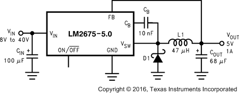
The LM2675 series of regulators are monolithic integrated DC-DC converter circuits built with a LMDMOS process. These regulators provide all the active functions for a step-down (buck) switching regulator, capable of driving a 1-A load current with excellent line and load regulation. These devices are available in fixed output voltages of 3.3 V, 5 V, 12 V, and an adjustable output version.
Requiring a minimum number of external components, these regulators are simple to use and include patented internal frequency compensation and a fixed frequency oscillator.
The LM2675 series operates at a switching frequency of 260 kHz, thus allowing smaller-sized filter components than what would be needed with lower frequency switching regulators. Because of its very high efficiency (>90%), the copper traces on the printed-circuit board are the only heat sinking needed.
Device Information(1)
| PART NUMBER | PACKAGE | BODY SIZE (NOM) |
|---|---|---|
| LM2675 | SOIC (8) | 5.00 mm × 6.20 mm |
| PDIP (8) | 10.16 mm × 6.60 mm | |
| WSON (16) | 5.00 mm × 5.00 mm |
- For all available packages, see the orderable addendum at the end of the data sheet.
Typical Application
