SNVS153F May 2001 – September 2016 LM2698
PRODUCTION DATA.
- 1 Features
- 2 Applications
- 3 Description
- 4 Revision History
- 5 Pin Configuration and Functions
- 6 Specifications
- 7 Detailed Description
- 8 Application and Implementation
- 9 Power Supply Recommendations
- 10Layout
- 11Device and Documentation Support
- 12Mechanical, Packaging, and Orderable Information
1 Features
- 1.9-A, 0.2-Ω Internal Switch (Typical)
- Operating Voltage as Low as 2.2 V
- 600 kHz to 1.25 MHz Adjustable Frequency Operation
- Switchers Made Simple® Software
- 8-Pin VSSOP Package
2 Applications
- 3.3 V to 5 V and 5 V to 12 V Conversion
- Distributed Power
- Set-Top Boxes
- DSL Modems
- Diagnostic Medical Instrumentation
- Boost Converters
- Flyback Converters
- SEPIC Converters
3 Description
The LM2698 device is a general purpose PWM boost converter. The 1.9-A, 18-V, 0.2-Ω internal switch enables the LM2698 to provide efficient power conversion to outputs ranging from 2.2 V to 17 V. It can operate with input voltages as low as 2.2 V and as high as 12 V. Current-mode architecture provides superior line and load regulation and simple frequency compensation over the device's 2.2 V to
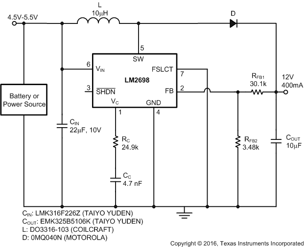
12 V input voltage range. The LM2698 sets the standard in power density and is capable of supplying 12 V at 400 mA from a 5-V input. The LM2698 can also be used in flyback or SEPIC topologies.
The LM2698 SIMPLE SWITCHER® features a pin selectable switching frequency of either 600 kHz or 1.25 MHz. This promotes flexibility in component selection and filtering techniques. A shutdown pin is available to suspend the device and decrease the quiescent current to 5 µA. An external compensation pin gives the user flexibility in setting frequency compensation, which makes possible the use of small, low-ESR ceramic capacitors at the output. Switchers Made Simple® software is available to ensure a quick, easy, and assured design. The LM2698 is available in a low-profile, 8-pin VSSOP (DGK) package.
Device Information(1)
| PART NUMBER | PACKAGE | BODY SIZE (NOM) |
|---|---|---|
| LM2698 | VSSOP (8) | 3.00 mm × 3.00 mm |
- For all available packages, see the orderable addendum at the end of the data sheet.
Typical Application Circuit
