SNOSD54 June 2017 LM339-MIL
PRODUCTION DATA.
1 Features
- Wide Supply Voltage Range
- 2 to 36 VDC or ±1 to ±18 VDC
- Very-Low Supply Current Drain (0.8 mA) — Independent of Supply Voltage
- Low Input Biasing Current: 25 nA
- Low Input Offset Current: ±5 nA
- Offset Voltage: ±3 mV
- Input Common-Mode Voltage Range Includes GND
- Differential Input Voltage Range Equal to the Power Supply Voltage
- Low Output Saturation Voltage: 250 mV at 4 mA
- Output Voltage Compatible With TTL, DTL, ECL, MOS, and CMOS Logic Systems
- Advantages:
- High-Precision Comparators
- Reduced VOS Drift Overtemperature
- Eliminates Need for Dual Supplies
- Allows Sensing Near GND
- Compatible With All Forms of Logic
- Power Drain Suitable for Battery Operation
2 Applications
- Limit Comparators
- Simple Analog-to-Digital Converters (ADCs)
- Pulse, Squarewave, and Time Delay Generators
- Wide Range VCO; MOS Clock Timers
- Multivibrators and High-Voltage Digital Logic Gates
3 Description
The LM339-MIL device consists of four independent precision voltage comparators with an offset voltage specification as low as 2 mV maximum for all four comparators. These comparators were designed specifically to operate from a single power supply over a wide range of voltages. Operation from split power supplies is also possible and the low-power supply current drain is independent of the magnitude of the power supply voltage. These comparators also have a unique characteristic in that the input common-mode voltage range includes ground, even though they are operated from a single power supply voltage.
The LM339-MIL device was designed to directly interface with TTL and CMOS. When operated from both plus and minus power supplies, the device directly interfaces with MOS logic where the low-power drain of the LM339-MIL is a distinct advantage over standard comparators.
Device Information(1)
| PART NUMBER | PACKAGE | BODY SIZE (NOM) |
|---|---|---|
| LM339-MIL | CDIP (14) | 19.56 mm × 6.67 mm |
| SOIC (14) | 8.65 mm × 3.91 mm | |
| PDIP (14) | 19.177 mm × 6.35 mm |
- For all available packages, see the orderable addendum at the end of the data sheet.
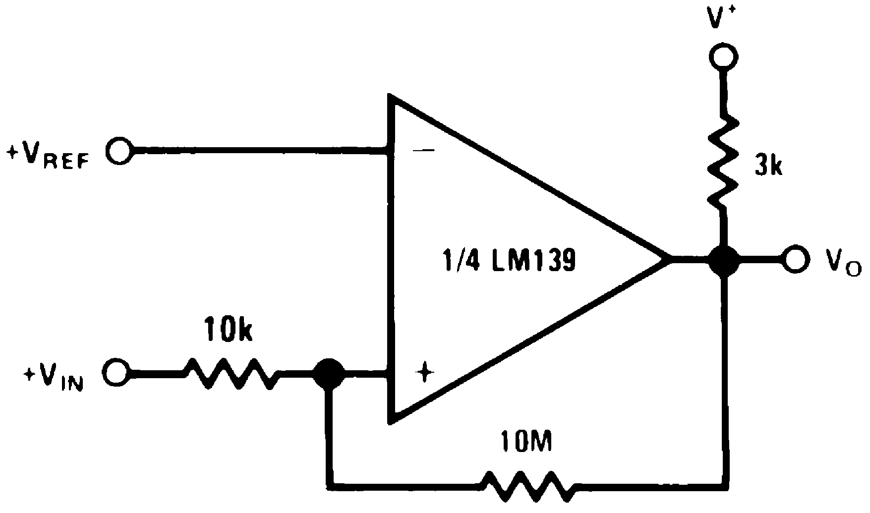
Noninverting Comparator With Hysteresis

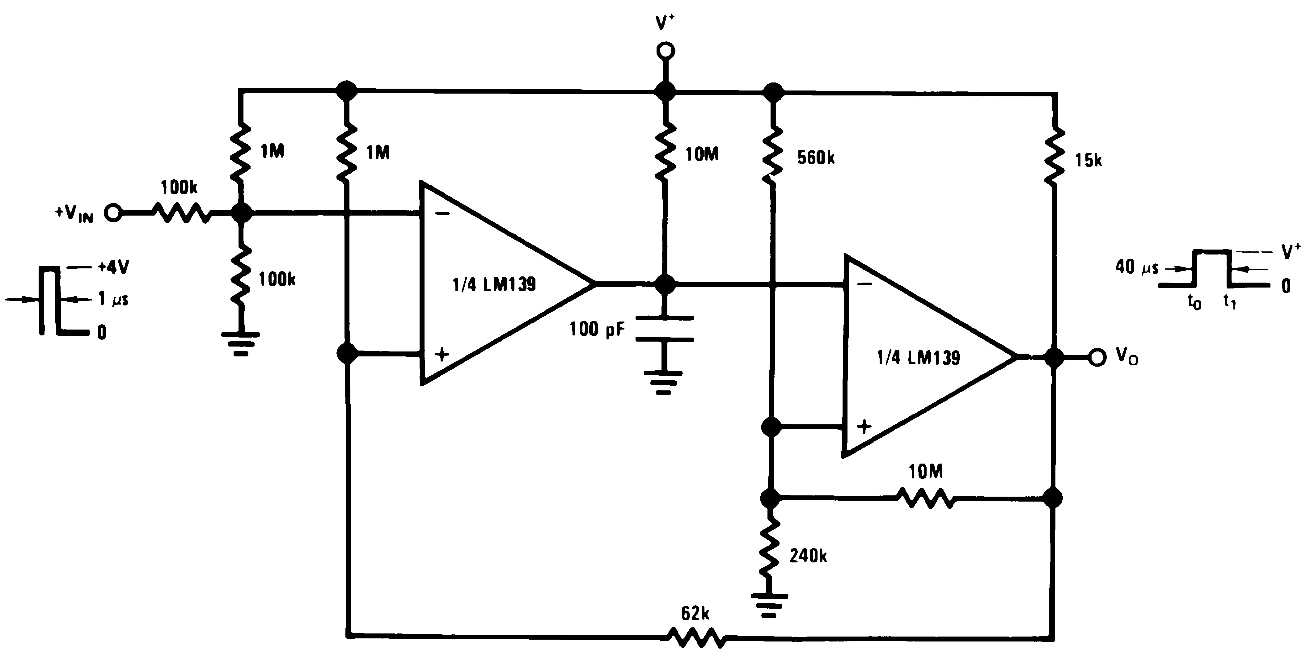
One-Shot Multivibrator With Input Lockout
