SNOS455G May 2000 – September 2015 LM4050-N , LM4050-N-Q1
PRODUCTION DATA.
- 1 Features
- 2 Applications
- 3 Description
- 4 Revision History
- 5 Pin Configuration and Functions
-
6 Specifications
- 6.1 Absolute Maximum Ratings
- 6.2 ESD Ratings
- 6.3 Recommended Operating Conditions
- 6.4 Thermal Information
- 6.5 Electrical Characteristics: 2-V Option
- 6.6 Electrical Characteristics: 2.5-V Option
- 6.7 Electrical Characteristics: 4.1-V Option
- 6.8 Electrical Characteristics: 5-V Option
- 6.9 Electrical Characteristics: 8.2-V Option
- 6.10 Electrical Characteristics: 10-V Option
- 6.11 Typical Characteristics
- 7 Parameter Measurement Information
- 8 Detailed Description
- 9 Application and Implementation
- 10Power Supply Recommendations
- 11Layout
- 12Device and Documentation Support
- 13Mechanical, Packaging, and Orderable Information
1 Features
- Small Package: SOT-23
- No Output Capacitor Required
- Tolerates Capacitive Loads
- Fixed Reverse Breakdown Voltages of 2.048 V, 2.5 V, 4.096 V, 5 V, 8.192 V, and 10 V
- Key Specifications (LM4050-N)
- Output Voltage Tolerance (A Grade, 25°C) ±0.1% (Maximum)
- Low Output Noise (10 Hz to 10 kHz) 41 μVrms (Typical)
- Wide Operating Current Range 60 μA to 15 mA
- Industrial Temperature Range −40°C to 85°C
- Extended Temperature Range −40°C to 125°C
- Low Temperature Coefficient 50 ppm/°C (max)
- LM4050-N-Q1 is AEC-Q100 Grade 1 Qualified and are Manufactured on an Automotive Grade Flow
2 Applications
- Portable, Battery-Powered Equipment
- Data Acquisition Systems
- Instrumentation
- Process Control
- Energy Management
- Product Testing
- Automotive
- Precision Audio Components
3 Description
Ideal for space-critical applications, the LM4050-N precision voltage reference is available in the sub-miniature (3 mm × 1.3 mm) SOT-23 surface-mount package. The LM4050-N design eliminates the need for an external stabilizing capacitor while ensuring stability with any capacitive load, thus making the LM4050-N easy to use. Further reducing design effort is the availability of several fixed reverse breakdown voltages: 2.048 V, 2.5 V, 4.096 V, 5 V, 8.192 V, and 10 V. The minimum operating current increases from 60 μA for the LM4050-N-2.0 to 100 μA for the LM4050-N-10.0. All versions have a maximum operating current of 15 mA.
The LM4050-N utilizes fuse and Zener-zap reverse breakdown voltage trim during wafer sort to ensure that the prime parts have an accuracy of better than ±0.1% (A grade) at 25°C. Bandgap reference temperature drift curvature correction and low dynamic impedance ensure stable reverse breakdown voltage accuracy over a wide range of operating temperatures and currents.
All grades and voltage options of the LM4050-N are available in both an industrial temperature range (−40°C and 85°C) and an extended temperature range (−40°C and 125°C).
Device Information(1)
| PART NUMBER | PACKAGE | BODY SIZE (NOM) |
|---|---|---|
| LM4050-N | SOT-23 (3) | 2.92 mm × 1.30 mm |
| LM4050-N-Q1 |
- For all available packages, see the orderable addendum at the end of the data sheet.
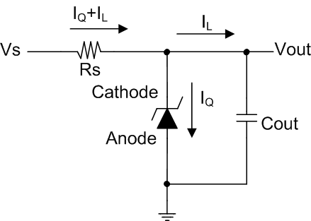
Shunt Regulator Schematic
