SNLS323N August 2010 – January 2017 LMH0395
PRODUCTION DATA.
- 1 Features
- 2 Applications
- 3 Description
- 4 Revision History
- 5 Pin Configuration and Functions
- 6 Specifications
-
7 Detailed Description
- 7.1 Overview
- 7.2 Functional Block Diagram
- 7.3 Feature Description
- 7.4 Device Functional Modes
- 7.5
Programming
- 7.5.1
SPI Register Access
- 7.5.1.1 SPI Transaction Overview
- 7.5.1.2 SPI Write
- 7.5.1.3 SPI Read
- 7.5.1.4 SPI Daisy-Chain Operation
- 7.5.1.5 SPI Daisy-Chain Write
- 7.5.1.6 SPI Daisy-Chain Read
- 7.5.1.7 SPI Daisy-Chain Read and Write Example
- 7.5.1.8 SPI Daisy-Chain Length Detection
- 7.5.1.9 Output Driver Adjustments and De-Emphasis Setting
- 7.5.1.10 Launch Amplitude Optimization
- 7.5.1.11 Cable Length Indicator (CLI)
- 7.5.1
SPI Register Access
- 7.6 Register Maps
- 8 Application and Implementation
- 9 Power Supply Recommendations
- 10Layout
- 11Device and Documentation Support
- 12Mechanical, Packaging, and Orderable Information
1 Features
- ST 424, ST 292, ST 344, ST 259, and DVB-ASI Compliant(6)
- Equalized Cable Lengths (Belden 1694A): 200 Meters at 2.97 Gbps, 220 Meters at 1.485 Gbps, and 400 Meters at 270 Mbps
- Ultra-low Power Consumption: 140 mW (Dual Outputs), 115 mW (Single Output)
- Dual Differential Outputs; Second Output Can Be Independently Powered Down
- Power-Save Mode With Auto Sleep Control (17-mW Typical Power Consumption in Power-Save Mode)
- Designed for Crosstalk Immunity
- Output De-Emphasis to Compensate for FR4 Board Trace Losses
- Digital and Analog Programmable MUTEREF Threshold
- Optional SPI Register Access and Pin Mode Operation
- Input Data Rates: 125 Mbps to 2.97 Gbps
- Internally Terminated 100-Ω LVDS Outputs With Programmable Output Common-Mode Voltage and Swing
- Programmable Launch Amplitude Optimization
- Cable Length Indicator
- Single 2.5-V Supply Operation
- 24-Pin WQFN Package
- Industrial Temperature Range: −40°C to +85°C
2 Applications
- ST 424, ST 292, ST 344, and ST 259 Serial Digital Interfaces(6)
- Broadcast Video Routers, Switchers, and Distribution Amplifiers
3 Description
The LMH0395 3-Gbps HD/SD SDI Dual Output Low Power Extended Reach Adaptive Cable Equalizer is designed to equalize data transmitted over cable (or any media with similar dispersive loss characteristics). The equalizer operates over a wide range of data rates from 125 Mbps to 2.97 Gbps and supports ST 424, ST 292, ST 344, ST 259, and DVB-ASI standards.
The LMH0395 device provides extended cable reach with improved immunity to crosstalk and ultra low power consumption. The equalizer includes active sensing circuitry that ensures robust performance and enhanced immunity to variations in the input signal launch amplitude. The LMH0395 offers power management to further reduce power consumption when no input signal is present.
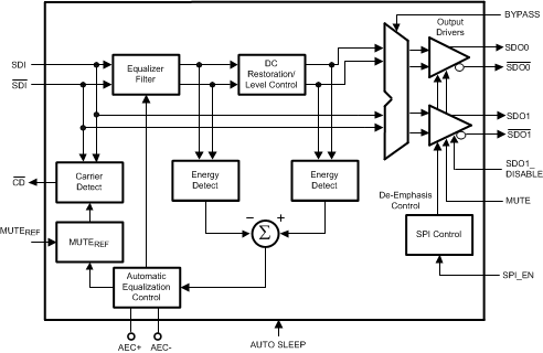
The LMH0395 has two differential serial data outputs, increasing flexibility and eliminating the need for a fanout buffer on the output in many applications. The outputs may be independently enabled and controlled. The output drivers offer programmable de-emphasis for up to 40 inches of FR4 trace losses. The LMH0395 supports two modes of operation. In pin mode, the LMH0395 operates with control pins to set its operating state. In SPI mode, an optional SPI serial interface can be used to access and configure multiple LMH0395 devices in a daisy-chain configuration.
Device Information(1)
| PART NUMBER | PACKAGE | BODY SIZE (NOM) |
|---|---|---|
| LMH0395 | WQFN (24) | 4.00 mm × 4.00 mm |
- For all available packages, see the orderable addendum at the end of the data sheet.
Functional Block Diagram

4 Revision History
Changes from M Revision (July 2015) to N Revision
- Changed MUTEREF pin description for both WQFN (Non-SPI) and WQFN SPI Mode packagesGo
- Changed sentence 'In pin mode, SPI_EN is driven logic low.' to 'Driving SPI_EN low enables pin mode.' to SPI Control descriptionGo
Changes from L Revision (April 2013) to M Revision
- Added Pin Configuration and Functions section, ESD Ratings table, Feature Description section, Device Functional Modes, Application and Implementation section, Power Supply Recommendations section, Layout section, Device and Documentation Support section, and Mechanical, Packaging, and Orderable Information section Go