SNOSA40K November 2002 – December 2016 LP2996-N , LP2996A
PRODUCTION DATA.
- 1 Features
- 2 Applications
- 3 Description
- 4 Revision History
- 5 Pin Configuration and Functions
- 6 Specifications
- 7 Detailed Description
- 8 Applications and Implementation
- 9 Power Supply Recommendations
- 10Layout
- 11Device and Documentation Support
- 12Mechanical, Packaging, and Orderable Information
封装选项
机械数据 (封装 | 引脚)
散热焊盘机械数据 (封装 | 引脚)
- DDA|8
订购信息
1 Features
- Minimum VDDQ:
- 1.8 V (LP2996-N)
- 1.35 V (LP2996A)
- Source and Sink Current
- Low Output Voltage Offset
- No External Resistors Required for Setting Output Voltage
- Linear Topology
- Suspend to Ram (STR) Functionality
- Stable With Ceramic Capacitors With Appropriate ESR
- Low External Component Count
- Thermal Shutdown
2 Applications
- LP2996-N: DDR1 and DDR2 Termination Voltage
- LP2996A: DDR1, DDR2, DDR3, and DDR3L Termination Voltage
- FPGA
- Industrial and Medical PC
- SSTL-2 and SSTL-3 Termination
- HSTL Termination
3 Description
The LP2996-N and LP2996A linear regulators are designed to meet the JEDEC SSTL-2 specifications for termination of DDR-SDRAM. The device also supports DDR2, while LP2996A supports DDR3 and DDR3L VTT bus termination with VDDQ minimum of 1.35 V. The device contains a high-speed operational amplifier to provide excellent response to load transients. The output stage prevents shoot through while delivering 1.5-A continuous current and transient peaks up to 3 A in the application as required for DDR-SDRAM termination. The LP2996-N and LP2996A also incorporate a VSENSE pin to provide superior load regulation and a VREF output as a reference for the chipset and DIMMs.
An additional feature found on the LP2996-N and LP2996A is an active-low shutdown (SD) pin that provides Suspend To RAM (STR) functionality. When SD is pulled low the VTT output will tri-state providing a high impedance output, but VREF remains active. A power savings advantage can be obtained in this mode through lower quiescent current.
TI recommends the LP2998 and LP2998-Q1 devices for automotive applications and DDR applications that require operating at temperatures below zero.
WEBENCH® design tools can be used by application designers to generate, optimize, and simlulate applications using the LP2998 and LP2998-Q1.
Device Information(1)
| PART NUMBER | PACKAGE | BODY SIZE (NOM) |
|---|---|---|
| LP2996-N | SOIC (8) | 4.90 mm x 3.90 mm |
| LP2996-N, LP2996A | WSON (8) | 4.90 mm x 3.90 mm |
| LP2996-N | WQFN (16) | 4.00 mm x 4.00 mm |
- For all available packages, see the orderable addendum at the end of the data sheet.
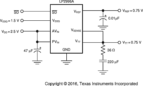
Simplified Schematic

4 Revision History
Changes from J Revision (March 2013) to K Revision
- Added Device Information table, Specifications section, ESD Ratings table, Thermal Information table, Feature Description section, Device Functional Modes section, Application and Implementation section, Power Supply Recommendations section, Layout section, Device and Documentation Support section, and Mechanical, Packaging, and Orderable Information sectionGo
- Added LP2996A throughout data sheetGo
- Added DDR3 support throughout data sheetGo
- Deleted Lead temperature (260°C maximum) from Absolute Maximum RatingsGo
- Changed Thermal Resistance, RθJA, values in Thermal Information From: 151°C/W To: 119.5°C/W (SOIC), From: 151°C/W To: 56.5°C/W (SO), and From: 151°C/W To: 52.7°C/W (WQFN)Go
Changes from I Revision (March 2013) to J Revision