SNVS185F February 2002 – April 2017 LP3982
PRODUCTION DATA.
- 1 Features
- 2 Applications
- 3 Description
- 4 Revision History
- 5 Pin Configuration and Functions
- 6 Specifications
- 7 Detailed Description
- 8 Application and Implementation
- 9 Power Supply Recommendations
- 10Layout
- 11Device and Documentation Support
- 12Mechanical, Packaging, and Orderable Information
1 Features
- 2.5-V to 6-V Input Range
- MAX8860 Pin, Package, and Specification Compatible
- 300-mA Output Current
- 120-mV Typical Dropout at 300 mA
- 90-μA Typical Quiescent Current
- 1-nA Typical Shutdown Mode
- 60-dB Typical PSRR
- 120-μs Typical Turnon Time
- Stable With Small Ceramic Output Capacitors
- 37-μVRMS Output Voltage Noise
(10 Hz to 100 kHz) - Overtemperature/Overcurrent Protection
- ±2% Output Voltage Tolerance
- Create a Custom Design Using the LP3982 With the WEBENCH® Power Designer
2 Applications
- Wireless Handsets
- DSP Core Power
- Battery Powered Electronics
- Portable Information Appliances
3 Description
The LP3982 low-dropout (LDO) CMOS linear regulator is available in 1.8-V, 2.5-V, 2.82-V, 3-V,
3.3-V, and adjustable versions. They deliver 300 mA of output current. Packaged in an 8-pin VSSOP, the LP3982 is pin- and package-compatible with Maxim's MAX8860. The LM3982 is also available in the small footprint WSON package.
The LP3982 suits battery-powered applications because of its shutdown mode (1 nA typical), low quiescent current (90 μA typical), and LDO voltage (120 mV typical). The low dropout voltage allows for more utilization of a battery’s available energy by operating closer to its end-of-life voltage. The LP3982 device's PMOS output transistor consumes relatively no drive current compared to PNP LDO regulators.
This PMOS regulator is stable with small ceramic capacitive loads (2.2 μF typical).
These devices also include regulation fault detection, a bandgap voltage reference, constant current limiting, and thermal-overload protection.
Device Information(1)
| PART NUMBER | PACKAGE | BODY SIZE (NOM) |
|---|---|---|
| LP3982 | WSON (8) | 2.50 mm × 3.00 mm |
| VSSOP (8) | 3.00 mm × 3.00 mm |
- For all available packages, see the orderable addendum at the end of the data sheet.
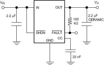
Application Circuit (Fixed VOUT Version)
