SCES587D AUGUST 2004 – November 2015 SN74AVCH16T245
PRODUCTION DATA.
- 1 Features
- 2 Applications
- 3 Description
- 4 Revision History
- 5 Description (continued)
- 6 Pin Configuration and Functions
-
7 Specifications
- 7.1 Absolute Maximum Ratings
- 7.2 ESD Ratings
- 7.3 Recommended Operating Conditions
- 7.4 Thermal Information
- 7.5 Electrical Characteristics
- 7.6 Switching Characteristics: VCCA = 1.2 V
- 7.7 Switching Characteristics: VCCA = 1.5 V ± 0.1 V
- 7.8 Switching Characteristics: VCCA = 1.8 V ± 0.15 V
- 7.9 Switching Characteristics: VCCA = 2.5 V ± 0.2 V
- 7.10 Switching Characteristics: VCCA = 3.3 V ± 0.3 V
- 7.11 Operating Characteristics
- 7.12 Typical Characteristics (TA = 25°C)
- 8 Parameter Measurement Information
- 9 Detailed Description
- 10Application and Implementation
- 11Power Supply Recommendations
- 12Layout
- 13Device and Documentation Support
- 14Mechanical, Packaging, and Orderable Information
封装选项
请参考 PDF 数据表获取器件具体的封装图。
机械数据 (封装 | 引脚)
- DGG|48
- DGV|48
散热焊盘机械数据 (封装 | 引脚)
订购信息
1 Features
- VCC Isolation Feature – If Either VCC Input is at GND, Both Ports are in the High-Impedance State
- Control Inputs VIH/VIL Levels Are Referenced to VCCA Voltage
- Overvoltage-Tolerant Inputs and Outputs Allow Mixed Voltage-Mode Data Communications
- Fully Configurable Dual-Rail Design Allows Each Port to Operate Over the Full 1.2 V to 3.6 V Power-Supply Range
- Ioff Supports Partial-Power-Down Mode Operation
- I/Os are 4.6 V Tolerant
- Bus Hold on Data Inputs Eliminates the Need for External Pullup and Pulldown Resistors
- Maximum Data Rates
- 380 Mbps (1.8 V to 3.3 V Level-Shifting)
- 200 Mbps (<1.8 V to 3.3 V Level-Shifting)
- 200 Mbps (Level-Shifting to 2.5 V or 1.8 V)
- 150 Mbps (Level-Shifting to 1.5 V)
- 100 Mbps (Level-Shifting to 1.2 V)
- Latch-Up Performance Exceeds 100 mA Per JESD 78, Class II
- ESD Protection Exceeds JESD 22
- 8000-V Human-Body Model (A114-A)
- 200-V Machine Model (A115-A)
- 1000-V Charged-Device Model (C101)
2 Applications
- Personal Electronics
- Industrial
- Enterprise
- Telecom
3 Description
This 16-bit noninverting bus transceiver uses two separate configurable power-supply rails. The SN74AVCH16T245 device is optimized to operate with VCCA/VCCB set at 1.4 V to 3.6 V. The device is operational with VCCA/VCCB as low as 1.2 V. The A port is designed to track VCCA. VCCA accepts any supply voltage from 1.2 V to 3.6 V. The B port is designed to track VCCB. VCCB accepts any supply voltage from 1.2 V to 3.6 V. This allows for universal low-voltage bidirectional translation between any of the 1.2-V, 1.5-V, 1.8-V, 2.5-V, and 3.3-V voltage nodes.
Device Information(1)
| PART NUMBER | PACKAGE | BODY SIZE (NOM) |
|---|---|---|
| SN74AVCH16T245 | TSSOP (48) | 12.50 mm × 6.10 mm |
| TVSOP (48) | 9.70 mm × 4.40 mm | |
| BGA MICROSTAR JUNIOR (56) | 7.00 mm × 4.50 mm |
- For all available packages, see the orderable addendum at the end of the data sheet.
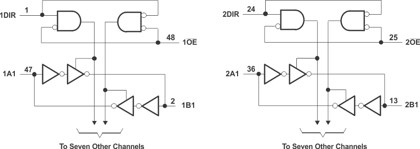
Logic Diagram (Positive Logic)
