SDLS146B October 1976 – September 2016 SN54LS245 , SN74LS245
- 1 Features
- 2 Applications
- 3 Description
- 4 Revision History
- 5 Device Comparison Table
- 6 Pin Configuration and Functions
- 7 Specifications
- 8 Parameter Measurement Information
- 9 Detailed Description
- 10Application and Implementation
- 11Power Supply Recommendations
- 12Layout
- 13Device and Documentation Support
- 14Mechanical, Packaging, and Orderable Information
封装选项
请参考 PDF 数据表获取器件具体的封装图。
机械数据 (封装 | 引脚)
- DB|20
- NS|20
- N|20
- DW|20
散热焊盘机械数据 (封装 | 引脚)
订购信息
1 Features
2 Applications
- Building Automation
- Electronic Point of Sale
- Factory Automation and Control
- Test and Measurement
3 Description
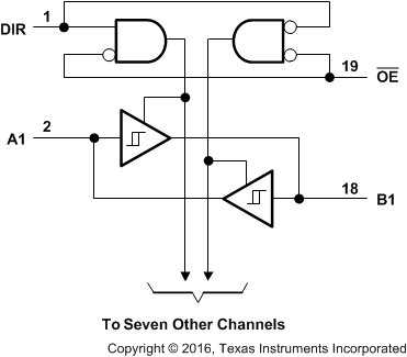
These octal bus transceivers are designed for asynchronous two-way communication between data buses. The control-function implementation minimizes external timing requirements.
The SNx4LS245 devices allow data transmission from the A bus to the B bus or from the B bus to the A bus, depending on the logic level at the direction-control (DIR) input. The output-enable (OE) input can disable the device so that the buses are effectively isolated.
Device Information(1)
| PART NUMBER | PACKAGE | BODY SIZE (NOM) |
|---|---|---|
| SN54LS245J | CDIP (20) | 24.20 mm × 6.92 mm |
| SN54LS245W | CFP (20) | 7.02 mm × 13.72 mm |
| SN54LS245FK | LCCC (20) | 8.89 mm × 8.89 mm |
| SN74LS245DB | SSOP (20) | 7.20 mm × 5.30 mm |
| SN74LS245DW | SOIC (20) | 12.80 mm × 7.50 mm |
| SN74LS245N | PDIP (20) | 24.33 mm × 6.35 mm |
| SN74LS245NS | SO (20) | 12.60 mm × 5.30 mm |
- For all available packages, see the orderable addendum at the end of the data sheet.
Logic Diagram (Positive Logic)
