SLOS626B December   2009  – November 2015 TPA2011D1

PRODUCTION DATA.  

  1. Features
  2. Applications
  3. Description
  4. Revision History
  5. Device Comparison Table
  6. Pin Configuration and Functions
  7. Specifications
    1. 7.1 Absolute Maximum Ratings
    2. 7.2 ESD Ratings
    3. 7.3 Recommended Operating Conditions
    4. 7.4 Thermal Information
    5. 7.5 Electrical Characteristics
    6. 7.6 Operating Characteristics
    7. 7.7 Dissipation Ratings
    8. 7.8 Typical Characteristics
  8. Parameter Measurement Information
  9. Detailed Description
    1. 9.1 Overview
    2. 9.2 Functional Block Diagram
    3. 9.3 Feature Description
      1. 9.3.1 Fully Differential Amplifier
        1. 9.3.1.1 Advantages of Fully Differential Amplifiers
      2. 9.3.2 Eliminating the Output Filter With the TPA2011D1
        1. 9.3.2.1 Effect on Audio
        2. 9.3.2.2 When to Use an Output Filter
      3. 9.3.3 Short Circuit Auto-Recovery
      4. 9.3.4 Integrated Image Reject Filter for DAC Noise Rejection
    4. 9.4 Device Functional Modes
      1. 9.4.1 Summing Input Signals With the TPA2011D1
        1. 9.4.1.1 Summing Two Differential Input Signals
        2. 9.4.1.2 Summing a Differential Input Signal and a Single-Ended Input Signal
        3. 9.4.1.3 Summing Two Single-Ended Input Signals
      2. 9.4.2 Shutdown Mode
  10. 10Application and Implementation
    1. 10.1 Application Information
    2. 10.2 Typical Applications
      1. 10.2.1 TPA2011D1 with Differential Input
        1. 10.2.1.1 Design Requirements
        2. 10.2.1.2 Detailed Design Procedure
          1. 10.2.1.2.1 Input Resistors (RI)
          2. 10.2.1.2.2 Decoupling Capacitor (CS)
        3. 10.2.1.3 Application Curves
      2. 10.2.2 TPA2011D1 with Differential Input and Input Capacitors
        1. 10.2.2.1 Design Requirements
        2. 10.2.2.2 Detailed Design Procedure
          1. 10.2.2.2.1 Input Capacitors (CI)
        3. 10.2.2.3 Application Curves
      3. 10.2.3 TPA2011D1 with Single-Ended Input
        1. 10.2.3.1 Design Requirements
        2. 10.2.3.2 Detailed Design Procedure
        3. 10.2.3.3 Application Curves
  11. 11Power Supply Recommendations
    1. 11.1 Power Supply Decoupling Capacitors
  12. 12Layout
    1. 12.1 Layout Guidelines
    2. 12.2 Layout Example
  13. 13Device and Documentation Support
    1. 13.1 Community Resources
    2. 13.2 Trademarks
    3. 13.3 Electrostatic Discharge Caution
    4. 13.4 Glossary
  14. 14Mechanical, Packaging, and Orderable Information

封装选项

机械数据 (封装 | 引脚)
散热焊盘机械数据 (封装 | 引脚)
订购信息

1 Features

  • Powerful Mono Class-D Amplifier
    • 3.24 W (4 Ω, 5 V, 10% THDN)
    • 2.57 W (4 Ω, 5 V, 1% THDN)
    • 1.80 W (8 Ω, 5 V, 10% THDN)
    • 1.46 W (8 Ω, 5 V, 1% THDN)
  • Integrated Feedback Resistor of 300 kΩ
  • Integrated Image Reject Filter for DAC Noise Reduction
  • Low Output Noise of 20 μV
  • Low Quiescent Current of 1.5 mA
  • Auto Recovering Short-Circuit Protection
  • Thermal Overload Protection
  • 9-Ball, 1.21mm x 1.16 mm 0.4 mm Pitch DSBGA

2 Applications

  • Wireless or Cellular Handsets and PDAs
  • Portable Navigation Devices
  • General Portable Audio Devices

3 Description

The TPA2011D1 is a 3.2-W high efficiency filter-free class-D audio power amplifier (class-D amp) in a 1.21 mm × 1.16 mm wafer chip scale package (DSBGA) that requires only three external components.

Features like 95% efficiency, 86-dB PSRR, 1.5 mA quiescent current and improved RF immunity make the TPA2011D1 class-D amp ideal for cellular handsets. A fast start-up time of 4 ms with no audible turn-on pop makes the TPA2011D1 ideal for PDA and smart-phone applications. The TPA2011D1 allows independent gain while summing signals from separate sources, and has a low 20 μV noise floor.

Device Information(1)

PART NUMBER PACKAGE BODY SIZE (NOM)
TPA2011D1 DSBGA (9) 1.60 mm x 1.21 mm
  1. For all available packages, see the orderable addendum at the end of the data sheet.

Typical Application Diagram
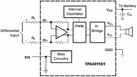
TPA2011D1 blk_los626.gif