SBVS149B September 2010 – January 2016 TPS386000-Q1
PRODUCTION DATA.
- 1 Features
- 2 Applications
- 3 Description
- 4 Revision History
- 5 Pin Configuration and Functions
- 6 Specifications
- 7 Parametric Measurement information
- 8 Detailed Description
- 9 Application and Implementation
- 10Power Supply Recommendations
- 11Layout
- 12Device and Documentation Support
- 13Mechanical, Packaging, and Orderable Information
1 Features
- Qualified for Automotive Applications
- AEC Q100 Test Guidance With the Following Results:
- Four Complete SVS Modules on one Silicon Platform
- Programmable Delay Time: 1.4 ms to 10 s
- Very Low Quiescent Current: 12 μA Typical
- Threshold Accuracy: 0.25% Typical
- SVS-1: Manual Reset (MR) Input
- SVS-1, 2, 3: Adjustable Threshold Down to 0.4 V
- SVS-4:
- Adjustable Threshold at Any Positive or Negative Voltage with VREF (1.2 V)
- Window Comparator
- Watchdog Timer with Dedicated Output
- Well-Controlled RESETn Output During Power-Up
- Open-Drain RESETn and WDO
- Package: 4-mm x 4-mm, 20-pin VQFN
2 Applications
- Automotive
- ADAS
- Front Camera, Surround View, Long-Range Radar, and Short-Range Radar
3 Description
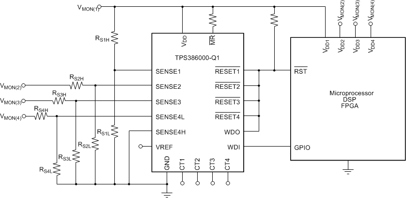
The TPS386000-Q1 family of voltage supervisors can monitor four power rails that are greater than 0.4 V and one power rail less than 0.4 V (including negative voltage) with a 0.25% (typical) threshold accuracy. Each of the four supervisory circuits (SVS-n) assert a RESETn or RESETn output signal when the SENSEm input voltage drops below the programmed threshold. With external resistors, the threshold of each SVS-n can be programmed (where n = 1, 2, 3, 4 and m = 1, 2, 3, 4L, 4H).
Each SVS-n has a programmable delay before releasing RESETn or RESETn. The delay time can be set from 1.4 ms to 10 s through the CTn pin connection. Only SVS-1 has an active-low manual reset (MR) input; a logic-low input to MR asserts RESET1 or RESET1.
SVS-4 monitors the threshold window using two comparators. The extra comparator can be configured as a fifth SVS to monitor negative voltage with voltage reference output VREF.
The TPS386000-Q1 device has a very low quiescent current of 12 μA (typical) and is available in a small, 4-mm x 4-mm, VQFN-20 package.
Device Information(1)
| PART NUMBER | PACKAGE | BODY SIZE (NOM) |
|---|---|---|
| TPS38600-Q1 | VQFN (20) | 4.00 mm × 4.00 mm |
- For all available packages, see the orderable addendum at the end of the datasheet.
TPS386000-Q1 Typical Application Circuit
