-
TPS63700 DC-DC Inverter
- 1 Features
- 2 Applications
- 3 Description
- 4 Revision History
- 5 Pin Configuration and Functions
- 6 Specifications
- 7 Detailed Description
- 8 Application and Implementation
- 9 Power Supply Recommendations
- 10Layout
- 11Device and Documentation Support
- 12Mechanical, Packaging, and Orderable Information
- IMPORTANT NOTICE
TPS63700 DC-DC Inverter
1 Features
- Adjustable Output Voltage Down to –15 V
- 2.7-V to 5.5-V Input Voltage Range
- Up to 360-mA Output Current
- 1000-mA Typical Switch Current Limit
- Up to 84% Efficiency
- Typical 1.4-MHz Fixed-Frequency PWM
Operation - Thermal Shutdown
- Typical –19-V Output Overvoltage Protection
- 1.5-μA Shutdown Current
- Small 3-mm × 3-mm SON-10 Package (DRC)
2 Applications
- Generic Negative Voltage Supply
- Small-to-Medium Size OLED Displays
- Bias Supply
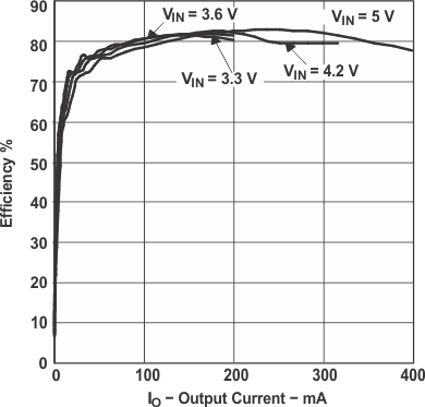
Efficiency vs Output Current

3 Description
The TPS63700 is an inverting DC/DC converter generating a negative output voltage down to –15 V with output currents up to 360 mA, depending on input-voltage to output-voltage ratio. With a peak efficiency of 84%, the device is ideal for portable battery-powered equipment. The input voltage range of 2.7 V to 5.5 V allows the TPS63700 to be directly powered from a Li-ion battery, from 3-cell NiMH/NiCd, from a 3.3-V or 5-V supply rail.
The inverter operates with a fixed-frequency pulse width modulation (PWM) control topology. The device has an internal current limit, overvoltage protection, and a thermal shutdown for highest reliability under fault conditions.
A switching frequency of typically 1.4 MHz allows the use of small external components enabling a small solution size.
The TPS63700 comes in a small 3-mm × 3-mm SON-10 package.
Device Information(1)
| PART NUMBER | PACKAGE | BODY SIZE (NOM) |
|---|---|---|
| TPS63700 | VSON (10) | 3.00 mm x 3.00 mm |
- For all available packages, see the orderable addendum at the end of the datasheet.
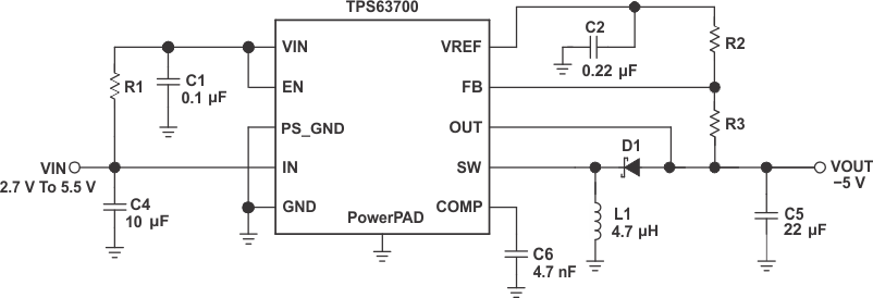
Typical Application Schematic
