SLVS667B July 2006 – January 2016 TPS65022
PRODUCTION DATA.
- 1 Features
- 2 Applications
- 3 Description
- 4 Revision History
- 5 Pin Configuration and Functions
- 6 Specifications
-
7 Detailed Description
- 7.1 Overview
- 7.2 Functional Block Diagram
- 7.3
Feature Description
- 7.3.1 VRTC Output and Operation With or Without Backup Battery
- 7.3.2 Step-Down Converters, VDCDC1, VDCDC2, and VDCDC3
- 7.3.3 Power Save Mode Operation
- 7.3.4 Low Ripple Mode
- 7.3.5 Soft-Start
- 7.3.6 100% Duty Cycle Low Dropout Operation
- 7.3.7 Active Discharge When Disabled
- 7.3.8 Power Good Monitoring
- 7.3.9 Low Dropout Voltage Regulators
- 7.3.10 Undervoltage Lockout
- 7.3.11 Power-Up Sequencing
- 7.3.12 System Reset + Control Signals
- 7.4 Device Functional Modes
- 7.5 Programming
- 7.6
Register Maps
- 7.6.1 VERSION Register Address: 00h (read only)
- 7.6.2 PGOODZ Register Address: 01h (read only)
- 7.6.3 MASK Register Address: 02h (read/write) Default Value: C0h
- 7.6.4 REG_CTRL Register Address: 03h (read/write) Default Value: FFh
- 7.6.5 CON_CTRL Register Address: 04h (read/write) Default Value: B1h
- 7.6.6 CON_CTRL2 Register Address: 05h (read/write) Default Value: 40h
- 7.6.7 DEFCORE Register Address: 06h (read/write) Default Value: 14h/1Eh
- 7.6.8 DEFSLEW Register Address: 07h (read/write) Default Value: 06h
- 7.6.9 LDO_CTRL Register Address: 08h (read/write) Default Value: set with DEFLDO1 and DEFLDO2
- 8 Application and Implementation
- 9 Power Supply Recommendations
- 10Layout
- 11Device and Documentation Support
- 12Mechanical, Packaging, and Orderable Information
1 Features
- 1.2-A, 97% Efficient Step-Down Converter for System Voltage (VDCDC1)
- 1-A, Up to 95% Efficient Step-Down Converter for Memory Voltage (VDCDC2)
- 900-mA, 90% Efficient Step-Down Converter for Processor Core (VDCDC3)
- 30-mA LDO and Switch for Real-Time Clock (VRTC)
- 2 × 200 mA General-Purpose LDO
- Dynamic Voltage Management for Processor Core
- Preselectable LDO Voltage Using Two Digital Input Pins
- Externally Adjustable Reset Delay Time
- Battery Backup Functionality
- Separate Enable Pins for Inductive Converters
- I2C Compatible Serial Interface
- 85-μA Quiescent Current
- Low Ripple PFM Mode
- Thermal Shutdown Protection
2 Applications
- PDA
- Cellular and Smart Phones
- Internet Audio Players
- Digital Still Cameras
- Digital Radio Players
- Split Supply TMS320™ DSP Family and μP Solutions:
OMAP™1610, OMAP1710, OMAP330, XScale Bulverde, Samsung ARM-Based Processors, and so forth - Intel® PXA270, and so forth
3 Description
The TPS65022 is an integrated Power Management IC for applications powered by one Li-Ion or Li-Polymer cell, and which require multiple power rails. The TPS65022 provides three highly efficient, step-down converters targeted at providing the core voltage, peripheral, I/O and memory rails in a processor based system.
All three step-down converters enter a low-power mode at light load for maximum efficiency across the widest possible range of load currents. The TPS65022 also integrates two general-purpose 200-mA LDO voltage regulators, which are enabled with an external input pin. Each LDO operates with an input voltage range between 1.5 V and 6.5 V, allowing them to be supplied from one of the step-down converters or directly from the battery.
The default output voltage of the LDOs can be digitally set to 4 different voltage combinations using the DEFLDO1 and DEFLDO2 pins.
The serial interface can be used for dynamic voltage scaling, masking interrupts, or for disabling, enabling, and setting the LDO output voltages. The interface is compatible with the Fast/Standard mode I2C specification, allowing transfers at up to 400 kHz. The TPS65022 is available in a 40-pin (RHA) VQFN package, and operates over a free-air temperature of –40°C to 85°C.
Device Information(1)
| PART NUMBER | PACKAGE | BODY SIZE (NOM) |
|---|---|---|
| TPS65022 | VQFN (40) | 6.00 mm × 6.00 mm |
- For all available packages, see the orderable addendum at the end of the data sheet.
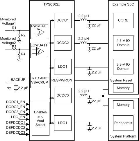
Simplified Schematic

4 Revision History
Changes from A Revision (July 2006) to B Revision
- Added ESD Ratings table, Feature Description section, Device Functional Modes, Application and Implementation section, Power Supply Recommendations section, Layout section, Device and Documentation Support section, and Mechanical, Packaging, and Orderable Information section.Go