SBVS034N September   2003  – December 2015 TPS731

PRODUCTION DATA.  

  1. Features
  2. Applications
  3. Description
  4. Revision History
  5. Pin Configuration and Functions
  6. Specifications
    1. 6.1 Absolute Maximum Ratings
    2. 6.2 ESD Ratings
    3. 6.3 Recommended Operating Conditions
    4. 6.4 Thermal Information
    5. 6.5 Electrical Characteristics
    6. 6.6 Typical Characteristics
  7. Detailed Description
    1. 7.1 Overview
    2. 7.2 Functional Block Diagrams
    3. 7.3 Feature Description
      1. 7.3.1 Output Noise
      2. 7.3.2 Internal Current Limit
      3. 7.3.3 Enable Pin and Shutdown
      4. 7.3.4 Reverse Current
    4. 7.4 Device Functional Modes
      1. 7.4.1 Normal Operation With 1.7 V ≤ VIN ≤ 5.5 V and VEN ≥ 1.7 V
  8. Application and Implementation
    1. 8.1 Application Information
    2. 8.2 Typical Applications
      1. 8.2.1 Design Requirements
      2. 8.2.2 Detailed Design Procedure
        1. 8.2.2.1 Input and Output Capacitor Requirements
        2. 8.2.2.2 Dropout Voltage
        3. 8.2.2.3 Transient Response
      3. 8.2.3 Application Curves
  9. Power Supply Recommendations
  10. 10Layout
    1. 10.1 Layout Guidelines
    2. 10.2 Layout Example
    3. 10.3 Thermal Considerations
      1. 10.3.1 Power Dissipation
  11. 11Device and Documentation Support
    1. 11.1 Device Support
      1. 11.1.1 Development Support
        1. 11.1.1.1 Spice Models
      2. 11.1.2 Device Nomenclature
    2. 11.2 Documentation Support
      1. 11.2.1 Related Documentation
    3. 11.3 Related Links
    4. 11.4 Community Resources
    5. 11.5 Trademarks
    6. 11.6 Electrostatic Discharge Caution
    7. 11.7 Glossary
  12. 12Mechanical, Packaging, and Orderable Information

封装选项

机械数据 (封装 | 引脚)
散热焊盘机械数据 (封装 | 引脚)
订购信息

1 Features

  • Stable With or Without Capacitors of All Types
  • Input Voltage Range of 1.7 V to 5.5 V
  • Ultralow Dropout Voltage: 30 mV Typical (150-mA Load)
  • Excellent Load Transient Response—With or Without Optional Output Capacitor
  • New NMOS Topology Provides Low Reverse Leakage Current
  • Low Noise: 30 μVRMS Typical (10 kHz to 100 kHz)
  • 0.5% Initial Accuracy
  • 1% Overall Accuracy Over Line, Load, and Temperature
  • Less Than 1-μA Maximum IQ in Shutdown Mode
  • Thermal Shutdown and Specified Minimum and Maximum Current Limit Protection
  • Available in Multiple Output Voltage Versions
    • Fixed Outputs of 1.20 V to 5 V
    • Adjustable Outputs from 1.2 V to 5.5 V
    • Custom Outputs Available

2 Applications

  • Smart Grid and Energy
  • Building Automation
  • Set-Top Boxes
  • Medical Equipment
  • Test and Measurement
  • Point-of-Sale Terminals
  • Wireless Infrastructure

3 Description

The TPS731xx family of low-dropout (LDO) linear voltage regulators uses a new topology: an NMOS pass element in a voltage-follower configuration. This topology is stable using output capacitors with low equivalent series resistance (ESR), and even allows operation without a capacitor. The device also provides high reverse blockage (low reverse current) and ground pin current that is nearly constant over all values of output current.

The TPS731xx uses an advanced BiCMOS process to yield high precision while delivering very low dropout voltages and low ground pin current. Current consumption, when not enabled, is less than 1 μA and ideal for portable applications. The extremely low output noise (30 μVRMS with 0.1-μF CNR) is ideal for powering VCOs. These devices are protected by thermal shutdown and foldback current limit.

Device Information(1)

PART NUMBER PACKAGE BODY SIZE (NOM)
TPS731xx SOT-23 (5) 2.90 mm × 1.60 mm
  1. For all available packages, see the orderable addendum at the end of the data sheet.

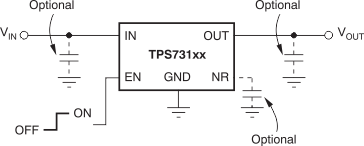
Typical Application Circuit for Fixed-Voltage Versions
TPS731 ac_front_bvs034.gif