SLVS720F June 2008 – November 2015
PRODUCTION DATA.
- 1 Features
- 2 Applications
- 3 Description
- 4 Revision History
- 5 Device Comparison Table
- 6 Pin Configuration and Functions
- 7 Specifications
- 8 Detailed Description
- 9 Application and Implementation
- 10Power Supply Recommendations
- 11Layout
- 12Device and Documentation Support
- 13Mechanical, Packaging, and Orderable Information
封装选项
机械数据 (封装 | 引脚)
散热焊盘机械数据 (封装 | 引脚)
- KTT|5
订购信息
1 Features
- Optimized for Fast Transient Response
- Output Current: 1.5 A
- High Output Voltage Accuracy: 1% at 25°C
- Dropout Voltage: 300 mV
- Low Noise: 35 μVRMS (10 Hz to 100 kHz)
- High Ripple Rejection: 68 dB at 1 kHz
- 1-mA Quiescent Current
- No Protection Diodes Needed
- Controlled Quiescent Current in Dropout
- Fixed Output Voltages: 1.5 V, 1.8 V, 2.5 V, 3.3 V
- Adjustable Output from 1.21 V to 20 V (TPS7A4501 Only)
- Less Than 1-μA Quiescent Current in Shutdown
- Stable With 10-μF Ceramic Output Capacitor
- Reverse-Battery Protection
- Reverse Current Protection
2 Applications
- Industrial
- Wireless Infrastructure
- Radio-Frequency Systems
3 Description
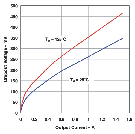
The TPS7A45xx devices are low-dropout (LDO) regulators optimized for fast transient response. The device can supply 1.5 A of output current with a dropout voltage of 300 mV. Operating quiescent current is 1 mA, dropping to less than 1 μA in shutdown. Quiescent current is well controlled; it does not rise in dropout as with many other regulators. In addition to fast transient response, the TPS7A45xx regulators have very-low output noise, which makes them ideal for sensitive RF supply applications.
Output voltage range is from 1.21 to 20 V. The TPS7A45xx regulators are stable with output capacitance as low as 10 μF. Small ceramic capacitors can be used without the necessary addition of ESR as is common with other regulators. Internal protection circuitry includes reverse-battery protection, current limiting, thermal limiting, and reverse-current protection. The devices are available in fixed output voltages of 1.5 V, 1.8 V, 2.5 V, 3.3 V, and as an adjustable device with a 1.21-V reference voltage.
Device Information(1)
| PART NUMBER | PACKAGE | BODY SIZE (NOM) |
|---|---|---|
| TPS7A45xx | SOT-223 (6) | 6.50 mm × 7.06 mm |
| TO-263 (5) | 10.16 mm × 15.24 mm |
- For all available packages, see the orderable addendum at the end of the data sheet.
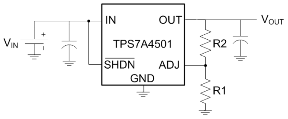
Simplified Schematic

Dropout Voltage vs Output Current
