SCDS261H March 2008 – June 2017 TS5A22364
PRODUCTION DATA.
- 1 Features
- 2 Applications
- 3 Description
- 4 Revision History
- 5 Pin Configuration and Functions
- 6 Specifications
- 7 Parameter Measurement Information
- 8 Detailed Description
- 9 Application and Implementation
- 10Power Supply Recommendations
- 11Layout
- 12Device and Documentation Support
- 13Mechanical, Packaging, and Orderable Information
封装选项
机械数据 (封装 | 引脚)
散热焊盘机械数据 (封装 | 引脚)
- DRC|10
订购信息
1 Features
- Specified Break-Before-Make Switching
- Negative Signaling Capability: Maximum Swing from –2.75 V to 2.75 V (VCC = 2.75 V)
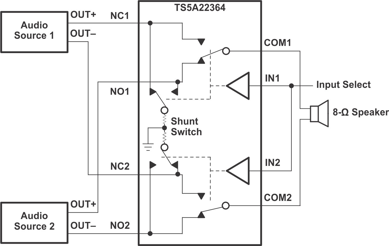
- Internal Shunt Switch Prevents Audible Click-and-Pop When Switching Between Two Sources
- Low ON-State Resistance (0.65 Ω Typical)
- Low Charge Injection
- Excellent ON-State Resistance Matching
- 2.3-V to 5.5-V Power Supply (VCC)
- Latch-Up Performance Exceeds 100 mA Per JESD 78, Class II
- ESD Performance Tested Per JESD 22
- 2500-V Human-Body Model
(A114-B, Class II) - 1500-V Charged-Device Model (C101)
- 200-V Machine Model (A115-A)
- 2500-V Human-Body Model
3 Description
The TS5A22364 is a bidirectional, 2-channel, single-pole double-throw (SPDT) analog switch designed to operate from 2.3 V to 5.5 V. The device features negative signal capability that allows signals below ground to pass through the switch without distortion. Additionally, the TS5A22364 includes an internal shunt switch, which automatically discharges any capacitance at the NC or NO terminals when they are unconnected to COM. This reduces the audible click/pop noise when switching between two sources. The break-before-make feature prevents signal distortion during the transferring of a signal from one path to another. Low ON-state resistance, excellent channel-to-channel ON-state resistance matching, and minimal total harmonic distortion (THD) performance are ideal for audio applications. The 3.00-mm x 3.00-mm DRC package is also available as a nonmagnetic package for medical imaging applications.
Device Information (1)
| PART NUMBER | PACKAGE | BODY SIZE (NOM) |
|---|---|---|
| TS5A22364 | VSON (10) | 3.00 mm × 3.00 mm |
| DSBGA (10) | 1.90 mm × 1.40 mm | |
| VSSOP (10) | 3.00 mm × 3.00 mm |
- For all available packages, see the orderable addendum at the end of the data sheet.
Typical Application Schematic
