SLLSE32G November 2010 – November 2017 TUSB1310A
PRODUCTION DATA.
- 1Device Overview
- 2Revision History
- 3Pin Configuration and Functions
- 4Specifications
-
5Detailed Description
- 5.1 Overview
- 5.2 Functional Block Diagram
- 5.3 Feature Description
- 5.4 Device Functional Modes
- 5.5
Register Maps
- 5.5.1 Vendor ID and Product ID (00h-03h)
- 5.5.2 Function Control (04h-06h)
- 5.5.3 Interface Control (07h-09h)
- 5.5.4 OTG Control
- 5.5.5 USB Interrupt Enable Rising (0Dh-0Fh)
- 5.5.6 USB Interrupt Enable Falling (10h-12h)
- 5.5.7 USB Interrupt Status (13h)
- 5.5.8 USB Interrupt Latch (14h)
- 5.5.9 Debug (15h)
- 5.5.10 Scratch Register (16-18h)
- 6Application, Implementation, and Layout
- 7Device and Documentation Support
- 8Mechanical, Packaging, and Orderable Information
1 Device Overview
1.1 Features
- Universal Serial Bus (USB)
- Single Port 5.0-Gbps USB 3.0 Physical Layer Transceiver
- One 5.0-Gbps SuperSpeed Connection
- One 480-Mbps HS/FS/LS Connection
- Fully Compliant With USB 3.0 Specification, Revision 1.0
- Supports 3+ Meters USB 3.0 Cable Length
- Fully Adaptive Equalizer to Optimize Receiver Sensitivity
- PIPE to Link-Layer Controller
- Supports 16-Bit SDR Mode at 250 MHz
- Compliant With PHY Interface for the USB Architectures (PIPE), Version 3.0
- ULPI to Link-Layer Controller
- Supports 8-Bit SDR Mode at 60 MHz
- Supports Synchronous Mode and Low-Power Mode
- Compliant With UTMI+ Low Pin Interface (ULPI) Specification, Revision 1.1
- Single Port 5.0-Gbps USB 3.0 Physical Layer Transceiver
- General Features
- IEEE 1149.1 JTAG Support
- IEEE 1149.6 JTAG support for the SuperSpeed Port
- Operates on One Reference Clock of 40 MHz
- 3.3-, 1.8-, and 1.1-V Supply Voltages
- 1.8-V PIPE and ULPI I/O
- Available in Lead-Free 175-Ball 12- × 12-nF NFBGA Package (ZAY)
1.2 Applications
- Surveillance Cameras
- Digital Still Cameras
- Multimedia Handsets
- Phones and Smartphones
- Portable Media Players
- Personal Navigation Devices
- Audio Docks
- Video- and Wireless-IP Phones
- Software Defined Radios
1.3 Description
The TUSB1310A device is one port, 5.0-Gbps USB 3.0 physical layer transceiver that operates off of one reference clock, which is provided by either a crystal or an external reference clock. The reference clock frequencies are selectable from 20, 25, 30, and 40 MHz. The TUSB1310A device provides the clock to the USB controller. The use of one reference clock allows the TUSB1310A device to provide a cost-effective USB 3.0 solution with few external components and a low implementation cost.
The USB controller interfaces to the TUSB1310A device through a PIPE (SuperSpeed) and a ULPI (USB 2.0) interface. The 16-bit PIPE operates off of a 250-MHz interface clock. The ULPI supports 8-bit operations with a 60-MHz interface clock.
USB 3.0 reduces active and idle power consumption with improved power-management features. The low-power states of the TUSB1310A device are controlled by the USB controller through the PIPE interface.
SuperSpeed USB uses existing USB software infrastructure by keeping the existing software interfaces and software drivers intact. In addition, SuperSpeed USB retains backward compatibility with USB 2.0 based products by using the same form-factor Type-A connector and cables. Existing USB 2.0 devices work with new USB 3.0 hosts and new USB 3.0 devices with work with legacy USB 2.0 hosts.
Device Information(1)
| PART NUMBER | PACKAGE | BODY SIZE (NOM) |
|---|---|---|
| TUSB1310A | NFBGA (175) | 12.00 mm × 12.00 mm |
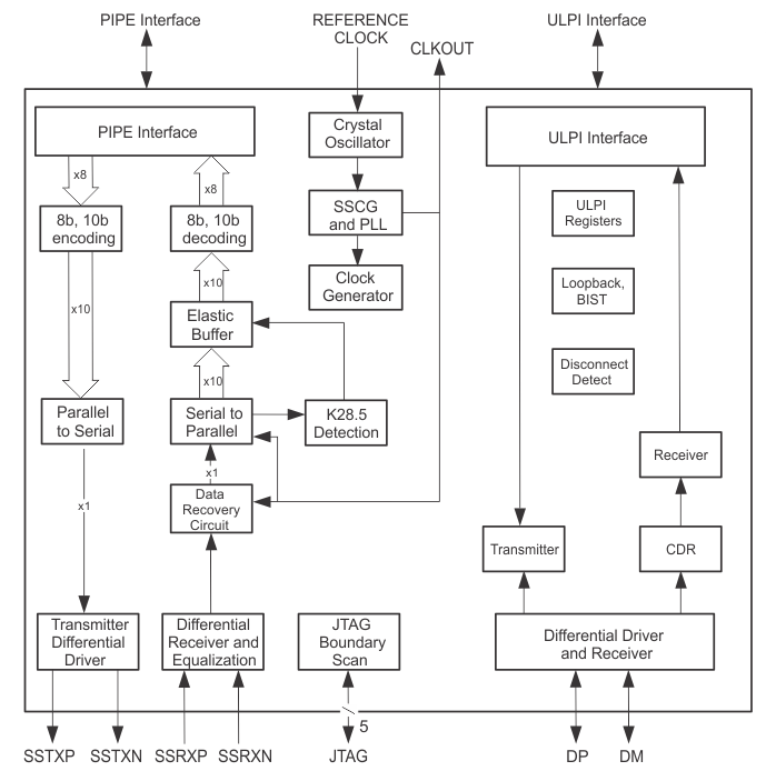
1.4 Functional Block Diagram
 Figure 1-1 Functional Block Diagram