SNLS488 March 2016 DS90UB921-Q1
PRODUCTION DATA.
- 1 Features
- 2 Applications
- 3 Description
- 4 Revision History
- 5 Pin Configuration and Functions
-
6 Specifications
- 6.1 Absolute Maximum Ratings
- 6.2 ESD Ratings - JEDEC
- 6.3 ESD Ratings—IEC and ISO
- 6.4 Recommended Operating Conditions
- 6.5 Thermal Information
- 6.6 DC Electrical Characteristics
- 6.7 AC Electrical Characteristics
- 6.8 PCLK Timing Requirements
- 6.9 Recommended Timing for the Serial Control Bus
- 6.10 Switching Characteristics
- 6.11 Typical Charateristics
-
7 Detailed Description
- 7.1 Overview
- 7.2 Functional Block Diagram
- 7.3
Feature Description
- 7.3.1 High Speed Forward Channel Data Transfer
- 7.3.2 Low Speed Back Channel Data Transfer
- 7.3.3 Common Mode Filter Pin (CMF)
- 7.3.4 Video Control Signal Filter
- 7.3.5 EMI Reduction Features
- 7.3.6 LVCMOS VDDIO Option
- 7.3.7 Power Down (PDB)
- 7.3.8 Remote Auto Power-Down Mode
- 7.3.9 Input PCLK Loss Detect
- 7.3.10 Serial Link Fault Detect
- 7.3.11 Pixel Clock Edge Select (TRFB)
- 7.3.12 Frequency Mode Optimizations
- 7.3.13 Interrupt Pins - Funtional Description and Usage (INTB, REM_INTB)
- 7.3.14 Internal Pattern Generation
- 7.3.15 GPIO[3:0] and GPO_REG[7:4]
- 7.3.16 I2S Transmitting
- 7.3.17 Built In Self Test (BIST)
- 7.4 Device Functional Modes
- 7.5 Programming
- 7.6 Register Maps
- 8 Application and Implementation
- 9 Power Supply Recommendations
- 10Layout
- 11Device and Documentation Support
- 12Mechanical, Packaging, and Orderable Information
Package Options
Mechanical Data (Package|Pins)
- RHS|48
Thermal pad, mechanical data (Package|Pins)
- RHS|48
Orderable Information
1 Features
- Qualified for Automotive Applications
- AEC-Q100 Qualified With the Following Results:
- Device Temperature Grade 2: -40℃ to +105℃ Ambient Operating Temperature Range
- Device HBM ESD Classification Level ±8kV
- Device CDM ESD Classification Level C6
- Supports Extended High Definition (1920x720p/60Hz) Digital Video Format
- 5 – 96MHz PCLK Supported (STP mode)
- 15 – 96MHz PCLK Supported (Coax mode)
- RGB888 + VS, HS, and DE
- Parallel LVCMOS Video Inputs
- Spread Spectrum Tolerant Input
- 4 Optional Bidirectional GPIO Channels
- Bidirectional Control Interface Channel Interface with I2C Compatible Serial Control Bus
- Optional I2S Support
- AC-Coupled Coax or STP Interconnect Up to 10 meters
- Single 3.3 V Operation with 1.8 V or 3.3 V Compatible LVCMOS I/O Interface
- DC-Balanced and Scrambled Data with Embedded Clock
- Internal Pattern Generation
- Low Power Modes Minimize Power Dissipation
- >8kV ISO 10605 ESD Rating
2 Applications
- Automotive Touch Screen Display
- Automotive Display for Navigation
- Automotive Instrument Cluster
3 Description
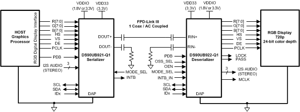
The DS90UB921-Q1 serializer, in conjunction with a DS90UB922-Q1, DS90UB926Q-Q1, DS90UB928Q-Q1, DS90UB948-Q1, or DS90UB940-Q1 deserializer, provides a complete digital interface for concurrent transmission of high-speed video, audio, and control data for automotive display and image sensing applications.
The chipset is ideally suited for automotive video-display systems with WVGA and HD formats. The DS90UB921-Q1 incorporates an embedded bidirectional control channel and low latency GPIO controls. This chipset translates a parallel interface into a single pair high-speed serialized interface. The serial bus scheme, FPD-Link III, supports full duplex of high-speed video data transmission and bidirectional control communication over a single link. Consolidation of video data and control over a single differential pair (or single wire) reduces the interconnect size and weight, while also eliminating skew issues and simplifying system design.
The DS90UB921-Q1 serializer embeds the clock, DC scrambles & balances the data payload, and level shifts the signals to high-speed low voltage differential (or single-ended) signaling. Up to 24 data bits are serialized along the video control signals.
EMI is minimized by the use of low voltage swing signaling, data scrambling and randomization and spread spectrum clocking compatibility.
Remote interrupts from the downstream deserializer are mirrored to a local output pin.
Device Information (1)
| PART NUMBER | PACKAGE | BODY SIZE (NOM) |
|---|---|---|
| DS90UB921-Q1 | WQFN (48) | 7.00 mm × 7.00 mm |
- For all available packages, see the orderable addendum at the end of the data sheet.
