SPRS866G November 2012 – October 2017 66AK2H06 , 66AK2H12 , 66AK2H14
PRODUCTION DATA.
- 1 Device Overview
- 2 Revision History
- 3 Device Comparison
- 4 Terminal Configuration and Functions
- 5 Specifications
- 6 C66x CorePac
- 7 ARM CorePac
- 8 Memory, Interrupts, and EDMA for 66AK2Hxx
- 9 System Interconnect
-
10Device Boot and Configuration
- 10.1
Device Boot
- 10.1.1 Boot Sequence
- 10.1.2
Boot Modes Supported
- 10.1.2.1 Boot Device Field
- 10.1.2.2 Device Configuration Field
- 10.1.2.3 Serial Rapid I/O Boot Device Configuration
- 10.1.2.4 Ethernet (SGMII) Boot Device Configuration
- 10.1.2.5
Boot Parameter Table
- 10.1.2.5.1 EMIF16 Boot Parameter Table
- 10.1.2.5.2 SRIO Boot Parameter Table
- 10.1.2.5.3 Ethernet Boot Parameter Table
- 10.1.2.5.4 PCIe Boot Parameter Table
- 10.1.2.5.5 I2C Boot Parameter Table
- 10.1.2.5.6 SPI Boot Parameter Table
- 10.1.2.5.7 HyperLink Boot Parameter Table
- 10.1.2.5.8 UART Boot Parameter Table
- 10.1.2.5.9 NAND Boot Parameter Table
- 10.1.2.5.10 DDR3 Configuration Table
- 10.1.2.6 Second-Level Bootloaders
- 10.1.3 SoC Security
- 10.1.4 System PLL Settings
- 10.2
Device Configuration
- 10.2.1 Device Configuration at Device Reset
- 10.2.2 Peripheral Selection After Device Reset
- 10.2.3
Device State Control Registers
- 10.2.3.1 Device Status (DEVSTAT) Register
- 10.2.3.2 Device Configuration Register
- 10.2.3.3 JTAG ID (JTAGID) Register Description
- 10.2.3.4 Kicker Mechanism (KICK0 and KICK1) Register
- 10.2.3.5 DSP Boot Address Register (DSP_BOOT_ADDRn)
- 10.2.3.6 LRESETNMI PIN Status (LRSTNMIPINSTAT) Register
- 10.2.3.7 LRESETNMI PIN Status Clear (LRSTNMIPINSTAT_CLR) Register
- 10.2.3.8 Reset Status (RESET_STAT) Register
- 10.2.3.9 Reset Status Clear (RESET_STAT_CLR) Register
- 10.2.3.10 Boot Complete (BOOTCOMPLETE) Register
- 10.2.3.11 Power State Control (PWRSTATECTL) Register
- 10.2.3.12 NMI Event Generation to C66x CorePac (NMIGRx) Register
- 10.2.3.13 IPC Generation (IPCGRx) Registers
- 10.2.3.14 IPC Acknowledgment (IPCARx) Registers
- 10.2.3.15 IPC Generation Host (IPCGRH) Register
- 10.2.3.16 IPC Acknowledgment Host (IPCARH) Register
- 10.2.3.17 Timer Input Selection Register (TINPSEL)
- 10.2.3.18 Timer Output Selection Register (TOUTPSEL)
- 10.2.3.19 Reset Mux (RSTMUXx) Register
- 10.2.3.20 Device Speed (DEVSPEED) Register
- 10.2.3.21 ARM Endian Configuration Register 0 (ARMENDIAN_CFGr_0), r=0..7
- 10.2.3.22 ARM Endian Configuration Register 1 (ARMENDIAN_CFGr_1), r=0..7
- 10.2.3.23 ARM Endian Configuration Register 2 (ARMENDIAN_CFGr_2), r=0..7
- 10.2.3.24 Chip Miscellaneous Control (CHIP_MISC_CTL0) Register
- 10.2.3.25 Chip Miscellaneous Control (CHIP_MISC_CTL1) Register
- 10.2.3.26 System Endian Status Register (SYSENDSTAT)
- 10.2.3.27 SYNECLK_PINCTL Register
- 10.2.3.28 USB PHY Control (USB_PHY_CTLx) Registers
- 10.1
Device Boot
-
1166AK2Hxx Peripheral Information
- 11.1 Recommended Clock and Control Signal Transition Behavior
- 11.2 Power Supplies
- 11.3 Power Sleep Controller (PSC)
- 11.4 Reset Controller
- 11.5
Main PLL, ARM PLL, DDR3A PLL, DDR3B PLL, PASS PLL and the PLL Controllers
- 11.5.1 Main PLL Controller Device-Specific Information
- 11.5.2
PLL Controller Memory Map
- 11.5.2.1 PLL Secondary Control Register (SECCTL)
- 11.5.2.2 PLL Controller Divider Register (PLLDIV3 and PLLDIV4)
- 11.5.2.3 PLL Controller Clock Align Control Register (ALNCTL)
- 11.5.2.4 PLLDIV Divider Ratio Change Status Register (DCHANGE)
- 11.5.2.5 SYSCLK Status Register (SYSTAT)
- 11.5.2.6 Reset Type Status Register (RSTYPE)
- 11.5.2.7 Reset Control Register (RSTCTRL)
- 11.5.2.8 Reset Configuration Register (RSTCFG)
- 11.5.2.9 Reset Isolation Register (RSISO)
- 11.5.3 Main PLL Control Registers
- 11.5.4 ARM PLL Control Registers
- 11.5.5 Main PLL Controller, ARM, SRIO, HyperLink, PCIe, USB Clock Input Electrical Data and Timing
- 11.6 DDR3A PLL and DDR3B PLL
- 11.7 PASS PLL
- 11.8 External Interrupts
- 11.9 DDR3A and DDR3B Memory Controllers
- 11.10 I2C Peripheral
- 11.11 SPI Peripheral
- 11.12 HyperLink Peripheral
- 11.13 UART Peripheral
- 11.14 PCIe Peripheral
- 11.15 Packet Accelerator
- 11.16 Security Accelerator
- 11.17 Network Coprocessor Gigabit Ethernet (GbE) Switch Subsystem
- 11.18 SGMII and XFI Management Data Input/Output (MDIO)
- 11.19 Ten-Gigabit Ethernet (10GbE) Switch Subsystem
- 11.20 Timers
- 11.21 Serial RapidIO (SRIO) Port
- 11.22 General-Purpose Input/Output (GPIO)
- 11.23 Semaphore2
- 11.24 Universal Serial Bus 3.0 (USB 3.0)
- 11.25 EMIF16 Peripheral
- 11.26 Emulation Features and Capability
- 11.27 Debug Port (EMUx)
- 12Device and Documentation Support
- 13Mechanical, Packaging, and Orderable Information
パッケージ・オプション
デバイスごとのパッケージ図は、PDF版データシートをご参照ください。
メカニカル・データ(パッケージ|ピン)
- AAW|1517
サーマルパッド・メカニカル・データ
発注情報
1 Device Overview
1.1 Features
- Eight TMS320C66x DSP Core Subsystems (C66x CorePacs), Each With
- 1.0 GHz or 1.2 GHz C66x Fixed- and Floating-Point DSP Core
- 38.4 GMacs/Core for Fixed Point @ 1.2 GHz
- 19.2 GFlops/Core for Floating Point @ 1.2 GHz
- Memory
- 32-KB L1P Per CorePac
- 32-KB L1D Per CorePac
- 1024-KB Local L2 Per CorePac
- 1.0 GHz or 1.2 GHz C66x Fixed- and Floating-Point DSP Core
- ARM CorePac
- Four ARM® Cortex®-A15 MPCore™ Processors at up to 1.4 GHz
- 4MB of L2 Cache Memory Shared by Four ARM Cores
- Full Implementation of ARMv7-A Architecture Instruction Set
- 32-KB L1 Instruction and Data Caches per Core
- AMBA 4.0 AXI Coherency Extension (ACE) Master Port, Connected to MSMC for Low-Latency Access to Shared MSMC SRAM
- Multicore Shared Memory Controller (MSMC)
- 6MB of MSM SRAM Memory Shared by Eight DSP CorePacs and One ARM CorePac
- Memory Protection Unit (MPU) for Both MSM SRAM and DDR3_EMIF
- Multicore Navigator
- 16k Multipurpose Hardware Queues With Queue Manager
- Packet-Based DMA for Zero-Overhead Transfers
- Network Coprocessor
- Packet Accelerator Enables Support for
- Transport Plane IPsec, GTP-U, SCTP, PDCP
- L2 User Plane PDCP (RoHC, Air Ciphering)
- 1-Gbps Wire Speed Throughput at 1.5 MPackets Per Second
- Security Accelerator Engine Enables Support for
- IPSec, SRTP, 3GPP, and WiMAX Air Interface, and SSL/TLS Security
- ECB, CBC, CTR, F8, A5/3, CCM, GCM, HMAC, CMAC, GMAC, AES, DES, 3DES, Kasumi, SNOW 3G, SHA-1, SHA-2 (256-Bit Hash), MD5
- Up to 2.4 Gbps IPSec and 2.4 Gbps Air Ciphering
- Ethernet Subsystem
- Five-Port Switch (Four SGMII Ports)
- Packet Accelerator Enables Support for
- Peripherals
- Four Lanes of SRIO 2.1
- Supports up to 5 GBaud
- Supports Direct I/O, Message Passing
- Two Lanes PCIe Gen2
- Supports up to 5 GBaud
- Two HyperLinks
- Supports Connections to Other KeyStone™ Architecture Devices Providing Resource Scalability
- Supports up to 50 GBaud
- 10-Gigabit Ethernet (10-GbE) Switch Subsystem (66AK2H14 Only)
- Two XFI Ports
- IEEE 1588 Support
- Five Enhanced Direct Memory Access (EDMA) Modules
- Two 72-Bit DDR3/DDR3L Interfaces With Speeds up to 1600 MHz
- EMIF16 Interface
- USB 3.0
- Two UART Interfaces
- Three I2C Interfaces
- 32 GPIO Pins
- Three SPI Interfaces
- Semaphore Module
- 64-Bit Timers
- Twenty 64-Bit Timers for 66AK2H14 and 66AK2H12
- Fourteen 64-Bit Timers for 66AK2H06
- Five On-Chip PLLs
- Four Lanes of SRIO 2.1
- Commercial Case Temperature:
- 0ºC to 85ºC
- Extended Case Temperature:
- –40ºC to 100ºC
1.2 Applications
- Mission Critical
- Computing
- Communications
- Audio
- Video Infrastructure
- Imaging
- Analytics
- Networking
- Media Processing
1.3 Description
The 66AK2Hxx platform combines the quad ARM Cortex-A15 processor with up to eight TMS320C66x high-performance DSPs using the KeyStone II architecture. The 66AK2H14/12/06 device provides up to 5.6 GHz of ARM and 9.6 GHz of DSP processing coupled with security, packet processing, and Ethernet switching at lower power than multichip solutions. The 66AK2H14/12/06 device is optimal for embedded infrastructure applications like cloud computing, media processing, high-performance computing, transcoding, security, gaming, analytics, and virtual desktop.
The C66x core combines fixed-point and floating-point computational capability in the processor without sacrificing speed, size, or power consumption. The raw computational performance is 38.4 GMACS/core and 19.2 Gflops/core (@ 1.2 GHz operating frequency). The C66x is also 100% backward compatible with software for C64x+ devices. The C66x core incorporates 90 new instructions targeted for floating point (FPi) and vector math oriented (VPi) processing.
The 66AK2H14/12/06 device has a complete set of development tools that includes: a C compiler, an assembly optimizer to simplify programming and scheduling, and a Windows® debugger interface for visibility into source code execution.
1.3.1 Enhancements in KeyStone II
The KeyStone II architecture provides many major enhancements over the previous KeyStone I generation of devices. The KeyStone II architecture integrates a Cortex-A15 processor quad-core cluster. The external memory bandwidth has been doubled with the integration of dual DDR3 1600 EMIFs. MSMC internal memory bandwidth is quadrupled with MSMC architecture improvements such as cache coherency. MSMC also enbles memories to operate at the speed of the processor cores, which reduces latency and contention while providing high-bandwidth interconnections between processor cores and shared internal and external memory. Multicore Navigator supports twice the number of queues, descriptors, and packet DMA, four times the number of micro RISC engines, and a significant increase in the number of push/pops per second compared to the previous generation. The new peripherals that have been added include the USB 3.0 controller, and asynchronous EMIF controller for NAND/NOR memory access. The 3-port Gigabit Ethernet switch in KeyStone I has been replaced with a 5-port Gigabit Ethernet switch in KeyStone II. Time synchronization support has been enhanced to reduce software workload and support additional standards like IEEE 1588 Annex D/E and SyncE. The number of GPIOs and serial interface peripherals, like I2C and SPI, have been increased to enable more board-level control functionality.
Device Information(1)
| PART NUMBER | PACKAGE | BODY SIZE |
|---|---|---|
| 66AK2H14 | AAW | 40.0 mm × 40.0 mm |
| 66AK2H12 | AAW | 40.0 mm × 40.0 mm |
| 66AK2H06 | AAW | 40.0 mm × 40.0 mm |
1.4 Functional Block Diagram
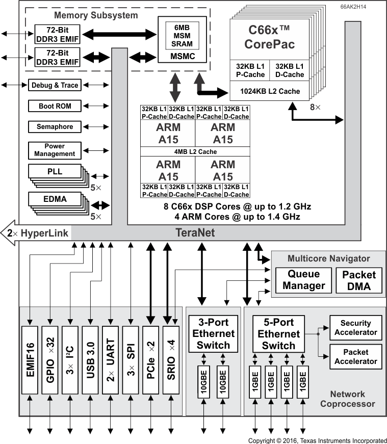
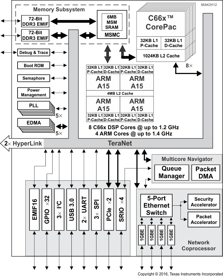
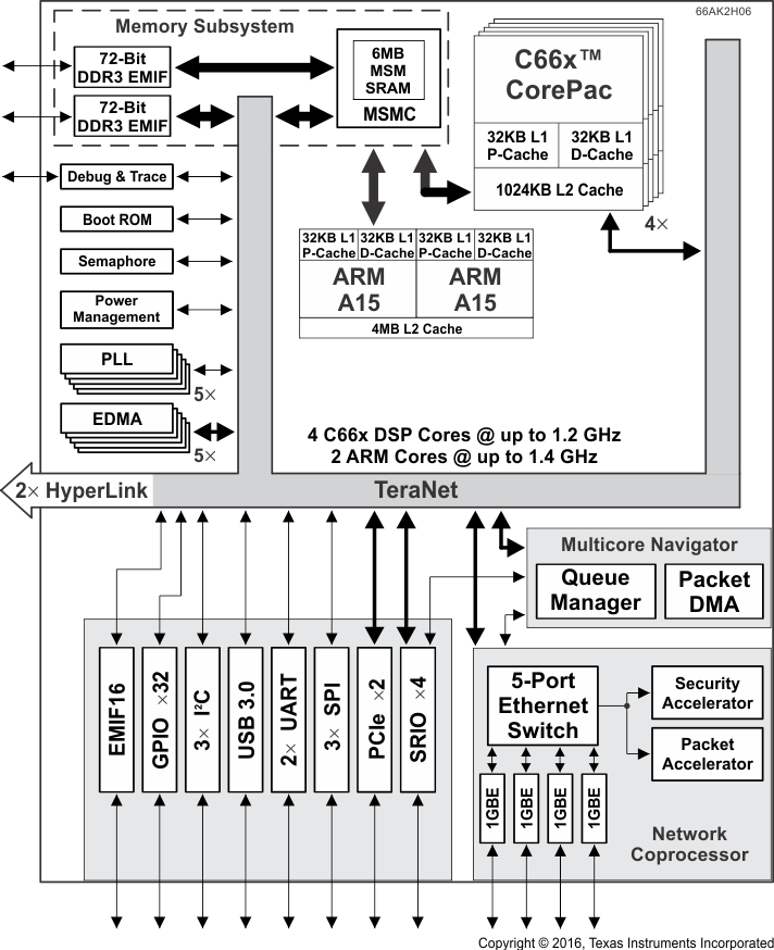
Figure 1-1, Figure 1-2, and Figure 1-3 show the functional block diagrams of the devices.
 Figure 1-1 Functional Block Diagram for 66AK2H14
 Figure 1-2 Functional Block Diagram for 66AK2H12
 Figure 1-3 Functional Block Diagram for 66AK2H06