SNLS250E May 2008 – April 2015 DP83848H , DP83848J , DP83848K , DP83848M , DP83848T
PRODUCTION DATA.
- 1Device Overview
- 2Revision History
- 3 Device Comparison
- 4Pin Configuration and Functions
- 5Specifications
-
6Detailed Description
- 6.1 Overview
- 6.2 Functional Block Diagram
- 6.3 Feature Description
- 6.4 Device Functional Modes
- 6.5
Programming
- 6.5.1
Architecture
- 6.5.1.1 100BASE-TX Transmitter
- 6.5.1.2
100BASE-TX Receiver
- 6.5.1.2.1 Analog Front End
- 6.5.1.2.2 Digital Signal Processor
- 6.5.1.2.3 Digital Adaptive Equalization and Gain Control
- 6.5.1.2.4 Base Line Wander Compensation
- 6.5.1.2.5 Signal Detect
- 6.5.1.2.6 MLT-3 to NRZI Decoder
- 6.5.1.2.7 NRZI to NRZ
- 6.5.1.2.8 Serial to Parallel
- 6.5.1.2.9 Descrambler
- 6.5.1.2.10 Code-Group Alignment
- 6.5.1.2.11 4B/5B Decoder
- 6.5.1.2.12 100BASE-TX Link Integrity Monitor
- 6.5.1.2.13 Bad SSD Detection
- 6.5.1.3
10BASE-T Transceiver Module
- 6.5.1.3.1 Operational Modes
- 6.5.1.3.2 Smart Squelch
- 6.5.1.3.3 Collision Detection and SQE
- 6.5.1.3.4 Carrier Sense
- 6.5.1.3.5 Normal Link Pulse Detection/Generation
- 6.5.1.3.6 Jabber Function
- 6.5.1.3.7 Automatic Link Polarity Detection and Correction
- 6.5.1.3.8 Transmit and Receive Filtering
- 6.5.1.3.9 Transmitter
- 6.5.1.3.10 Receiver
- 6.5.1
Architecture
- 6.6
Memory
- 6.6.1
Register Block
- 6.6.1.1
Register Definition
- 6.6.1.1.1 Basic Mode Control Register (BMCR)
- 6.6.1.1.2 Basic Mode Status Register (BMSR)
- 6.6.1.1.3 PHY Identifier Register #1 (PHYIDR1)
- 6.6.1.1.4 PHY Identifier Register #2 (PHYIDR2)
- 6.6.1.1.5 Auto-Negotiation Advertisement Register (ANAR)
- 6.6.1.1.6 Auto-Negotiation Link Partner Ability Register (ANLPAR) (BASE Page)
- 6.6.1.1.7 Auto-Negotiation Link Partner Ability Register (ANLPAR) (Next Page)
- 6.6.1.1.8 Auto-Negotiate Expansion Register (ANER)
- 6.6.1.1.9 Auto-Negotiation Next Page Transmit Register (ANNPTR)
- 6.6.1.2
Extended Registers
- 6.6.1.2.1 PHY Status Register (PHYSTS)
- 6.6.1.2.2 False Carrier Sense Counter Register (FCSCR)
- 6.6.1.2.3 Receiver Error Counter Register (RECR)
- 6.6.1.2.4 100 Mb/s PCS Configuration and Status Register (PCSR)
- 6.6.1.2.5 RMII and Bypass Register (RBR)
- 6.6.1.2.6 LED Direct Control Register (LEDCR)
- 6.6.1.2.7 PHY Control Register (PHYCR)
- 6.6.1.2.8 10BASE-T Status/Control Register (10BTSCR)
- 6.6.1.2.9 CD Test and BIST Extensions Register (CDCTRL1)
- 6.6.1.2.10 Energy Detect Control (EDCR)
- 6.6.1.1
Register Definition
- 6.6.1
Register Block
- 7Application, Implementation, and Layout
- 8Device and Documentation Support
- 9Mechanical Packaging and Orderable Information
パッケージ・オプション
メカニカル・データ(パッケージ|ピン)
- RTA|40
サーマルパッド・メカニカル・データ
- RTA|40
発注情報
1 Device Overview
1.1 Features
- Low-Power 3.3-V, 0.18-µm CMOS Technology
- Auto-MDIX for 10/100 Mb/s
- Energy Detection Mode
- 3.3-V MAC Interface
- RMII Rev. 1.2 Interface (configurable)
- MII Interface
- MII Serial Management Interface (MDC and MDIO)
- IEEE 802.3 Auto-Negotiation and Parallel Detection
- IEEE 802.3 ENDEC, 10BASE-T Transceivers and Filters
- IEEE 802.3 PCS, 100BASE-TX Transceivers and Filters
- Integrated ANSI X3.263 Compliant TP-PMD Physical Sub-Layer with Adaptive Equalization and Baseline Wander Compensation
- Error-Free Operation Beyond 137 Meters
- ESD Protection – Greater than 4 kV Human Body Model
- Configurable LED for Link and Activity (DP83848J/K)
- 25-MHz Clock Output (DP83848H/M/T)
- Single Register Access for Complete PHY Status
- 10/100 Mb/s Packet BIST (Built-in Self Test)
1.2 Applications
- Peripheral Devices
- Mobile Devices
- Factory and Building Automation
- Base Stations
1.3 Description
The DP83848x device addresses the quality, reliability and small form factor required for space sensitive applications in embedded systems.
The DP83848x offers performance far exceeding the IEEE specifications, with superior interoperability and industry leading performance beyond 137 meters of Cat-V cable. The DP83848x also offers Auto-MDIX to remove cabling complications. DP83848x has superior ESD protection, greater than 4 kV Human Body Model, providing extremely high reliability and robust operation, ensuring a high-level performance in all applications.
DP83848J/K offers two flexible LED indicators one for Link and the other for Speed. In addition, both MII and RMII are supported ensuring ease and flexibility of design.
The DP83848H/M/T incorporates a 25-MHz clock out that eliminates the need and hence the space and cost, of an additional clock source component.
The DP83848x is offered in small 6-mm × 6-mm WQFN 40-pin package and is ideal for industrial controls, building/factory automation, transportation, test equipment and wire-less base stations.
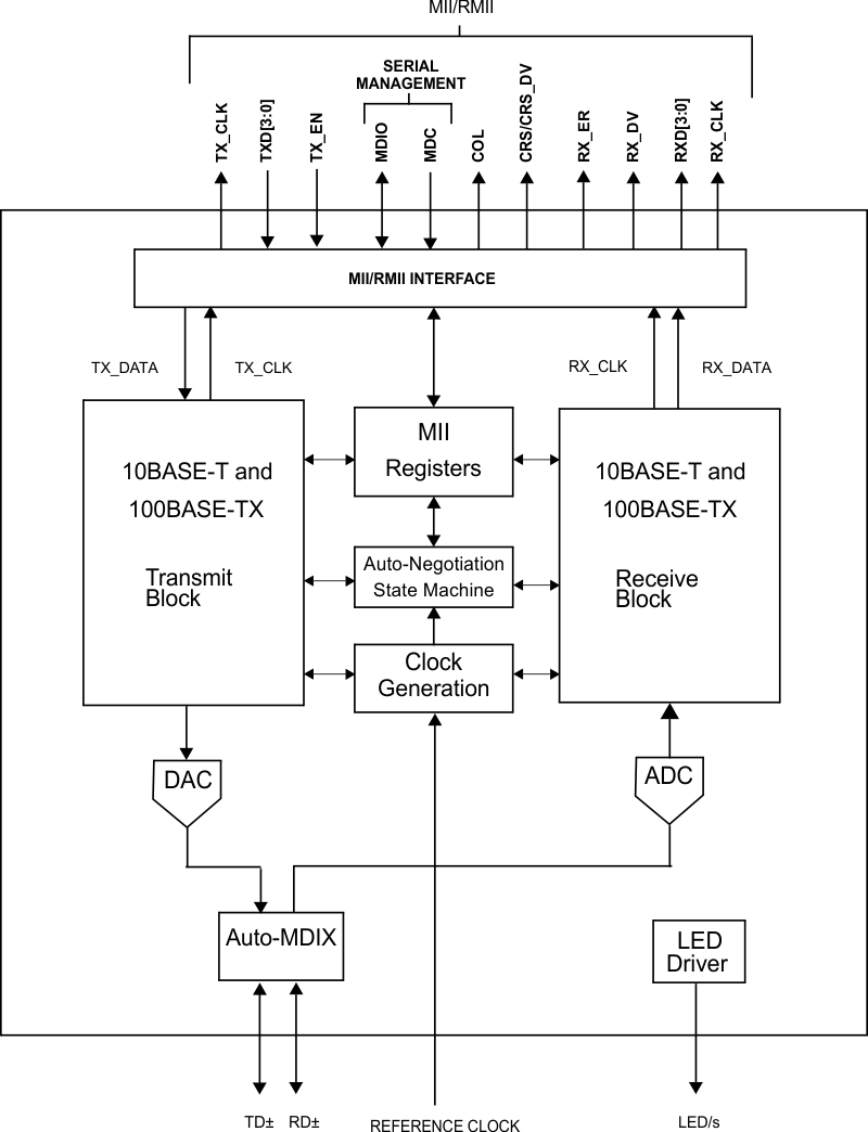
1.4 Functional Block Diagram
