SLOS846C September 2013 – December 2016 DRV8303
PRODUCTION DATA.
- 1 Features
- 2 Applications
- 3 Description
- 4 Revision History
- 5 Pin Configuration and Functions
-
6 Specifications
- 6.1 Absolute Maximum Ratings
- 6.2 ESD Ratings
- 6.3 Recommended Operating Conditions
- 6.4 Thermal Information
- 6.5 Electrical Characteristics
- 6.6 Current Shunt Amplifier Characteristics
- 6.7 SPI Characteristics (Slave Mode Only)
- 6.8 Gate Timing and Protection Switching Characteristics
- 6.9 Typical Characteristics
- 7 Detailed Description
- 8 Application and Implementation
- 9 Power Supply Recommendations
- 10Layout
- 11Device and Documentation Support
- 12Mechanical, Packaging, and Orderable Information
パッケージ・オプション
メカニカル・データ(パッケージ|ピン)
- DCA|48
サーマルパッド・メカニカル・データ
- DCA|48
発注情報
1 Features
- 6-V to 60-V Operating Supply Voltage Range
- 1.7-A Source and 2.3-A Sink Gate Drive Current Capability
- Slew Rate Control for EMI Reduction
- Bootstrap Gate Driver With 100% Duty Cycle Support
- 6 or 3 PWM Input Modes
- Dual Integrated Current-Shunt Amplifiers With Adjustable Gain and Offset
- 3.3-V and 5-V Interface Support
- Serial Peripheral Interface (SPI)
- Protection Features:
- Programmable Dead Time Control (DTC)
- Programmable Overcurrent Protection (OCP)
- PVDD and GVDD Undervoltage Lockout (UVLO)
- GVDD Overvoltage Lockout (OVLO)
- Overtemperature Warning/Shutdown (OTW/OTS)
- Reported through nFAULT, nOCTW, and SPI Registers
2 Applications
- 3-Phase BLDC and PMSM Motors
- CPAP and Pump
- E-Bikes
- Power Tools
- Robotics and RC Toys
- Industrial Automation
3 Description
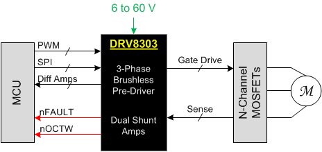
The DRV8303 is a gate driver IC for three-phase motor-drive applications. The device provides three half bridge drivers, each capable of driving two N-channel MOSFETs. The device supports up to 1.7-A source and 2.3-A peak current capability. The DRV8303 can operate off of a single power supply with a wide range from 6-V to 60-V. It uses a bootstrap gate-driver architecture with trickle charge circuitry to support 100% duty cycle. The DRV8303 uses automatic hand shaking when the high-side or low-side MOSFET is switching to prevent current shoot through. Integrated VDS sensing of the high-side and low-side MOSFETs is used to protect the external power stage against overcurrent conditions.
The DRV8303 includes two current-shunt amplifiers for accurate current measurement. The amplifiers support bi-directional current sensing and provide and adjustable output offset up to 3 V.
The serial peripheral interface (SPI) provides detailed fault reporting and flexible parameter settings such as gain options for the current-shunt amplifiers and slew-rate control of the gate drivers.
Device Information(1)
| PART NUMBER | PACKAGE | BODY SIZE (NOM) |
|---|---|---|
| DRV8303 | TSSOP (48) | 12.50 mm × 6.10 mm |
- For all available packages, see the orderable addendum at the end of the data sheet.
