SLLSE89G September 2011 – January 2015 ISO7640FM , ISO7641FM
UNLESS OTHERWISE NOTED, this document contains PRODUCTION DATA.
- 1 Features
- 2 Applications
- 3 Description
- 4 Revision History
- 5 Pin Configuration and Functions
-
6 Specifications
- 6.1 Absolute Maximum Ratings
- 6.2 ESD Ratings
- 6.3 Recommended Operating Conditions
- 6.4 Thermal Information
- 6.5 Electrical Characteristics: VCC1 and VCC2 at 5 V ±10%
- 6.6 Electrical Characteristics: VCC1 at 5 V ±10% and VCC2 at 3.3 V ±10%
- 6.7 Electrical Characteristics: VCC1 at 3.3 V ±10% and VCC2 at 5 V ±10%
- 6.8 Electrical Characteristics: VCC1 and VCC2 at 3.3 V ±10%
- 6.9 Electrical Characteristics: VCC1 and VCC2 at 2.7 V
- 6.10 Supply Current: VCC1 and VCC2 at 5 V ±10%
- 6.11 Supply Current: VCC1 at 5 V ±10% and VCC2 at 3.3 V ±10%
- 6.12 Supply Current: VCC1 at 3.3 V ±10% and VCC2 at 5 V ±10%
- 6.13 Supply Current: VCC1 and VCC2 at 3.3 V ±10%
- 6.14 Supply Current: VCC1 and VCC2 at 2.7 V
- 6.15 Switching Characteristics: VCC1 and VCC2 at 5 V ±10%
- 6.16 Switching Characteristics: VCC1 at 5 V ±10% and VCC2 at 3.3 V ±10%
- 6.17 Switching Characteristics: VCC1 at 3.3 V ±10% and VCC2 at 5 V ±10%
- 6.18 Switching Characteristics: VCC1 and VCC2 at 3.3 V ±10%
- 6.19 Switching Characteristics: VCC1 and VCC2 at 2.7 V
- 6.20 Typical Characteristics
- 7 Parameter Measurement Information
- 8 Detailed Description
- 9 Application and Implementation
- 10Power Supply Recommendations
- 11Layout
- 12Device and Documentation Support
- 13Mechanical, Packaging, and Orderable Information
パッケージ・オプション
メカニカル・データ(パッケージ|ピン)
- DW|16
サーマルパッド・メカニカル・データ
- DW|16
発注情報
1 Features
- Signaling Rate: 150 Mbps
- Low Power Consumption, Typical ICC per Channel (3.3-V Supplies):
- Low Propagation Delay: 7-ns Typical
- Output Defaults to Low-State in Fail-Safe Mode
- Wide Temperature Range: –40°C to 125°C
- 50-KV/µs Transient Immunity, Typical
- Long Life With SiO2 Isolation Barrier
- Operates From 2.7-V, 3.3-V, and 5-V Supply and Logic Levels
- Wide Body SOIC-16 Package
- Safety and Regulatory Approvals
- 6000 VPK / 4243 VRMS for 1 Minute per UL 1577
- VDE 6000 VPK Transient Overvoltage, 1414 VPK Working Voltage per DIN V VDE V 0884-10 (VDE V 0884-10):2006-12
- CSA Component Acceptance Notice 5A, IEC 60950-1, IEC 61010-1, and IEC 60601-1 End Equipment Standards
- TUV 5 KVRMS Reinforced Insulation per EN/UL/CSA 60950-1 and EN/UL/CSA 61010-1
- CQC Reinforced Insulation per GB4943.1-2011
2 Applications
- Optocoupler Replacement in:
- Industrial Fieldbus
- Profibus
- Modbus
- DeviceNet™ Data Buses
- Servo Control Interface
- Motor Control
- Power Supplies
- Battery Packs
- Industrial Fieldbus
3 Description
ISO7640FM and ISO7641FM provide galvanic isolation up to 6 KVPK for 1 minute per UL and VDE. These devices are also certified up to 5-KVRMS Reinforced isolation at a working voltage of 400 VRMS per end equipment standards EN/UL/CSA 60950-1 and 61010-1. ISO7640F and ISO7641F are quad-channel isolators; ISO7640F has four forward and ISO7641F has three forward and one reverse-direction channels. Suffix F indicates that output defaults to Low-state in fail-safe conditions (see Table 4). M-Grade devices are high-speed isolators capable of 150-Mbps data rate with fast propagation delays.
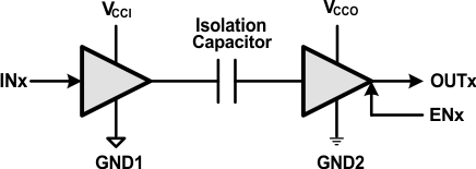
Each isolation channel has a logic input and output buffer separated by a silicon dioxide (SiO2) insulation barrier. Used in conjunction with isolated power supplies, these devices prevent noise currents on a data bus or other circuits from entering the local ground and interfering with or damaging sensitive circuitry. The devices have TTL input thresholds and can operate from 2.7-V, 3.3-V, and 5-V supplies. All inputs are 5-V tolerant when supplied from 3.3-V or 2.7-V supplies.
Device Information(1)
| PART NUMBER | PACKAGE | BODY SIZE (NOM) |
|---|---|---|
| ISO7640FM | SOIC (16) | 10.30 mm × 7.50 mm |
| ISO7641FM |
- For all available packages, see the orderable addendum at the end of the data sheet.
Simplified Schematic
