SNVS829E March 1999 – February 2017 LMP8480 , LMP8481
PRODUCTION DATA.
- 1 Features
- 2 Applications
- 3 Description
- 4 Revision History
- 5 Device Comparison Table
- 6 Pin Configuration and Functions
- 7 Specifications
-
8 Detailed Description
- 8.1 Overview
- 8.2 Functional Block Diagrams
- 8.3
Feature Description
- 8.3.1 Basic Connections
- 8.3.2 Selection of the Sense Resistor
- 8.3.3 Using PCB Traces as Sense Resistors
- 8.3.4 VREFA and VREFB Pins (LMP8481 Only)
- 8.3.5 Reference Input Voltage Limits (LMP8481 Only)
- 8.3.6 Low-Side Current Sensing
- 8.3.7 Input Series Resistance
- 8.3.8 Minimum Output Voltage
- 8.3.9 Swinging Output Below Ground
- 8.3.10 Maximum Output Voltage
- 8.4 Device Functional Modes
- 9 Application and Implementation
- 10Power Supply Recommendations
- 11Layout
- 12Device and Documentation Support
- 13Mechanical, Packaging, and Orderable Information
1 Features
- Typical Values: TA = 25°C
- Bidirectional or Unidirectional Sensing
- Common Mode Voltage Range: 4.0 V to 76 V
- Supply Voltage Range: 4.5 V to 76 V
- Fixed Gains: 20, 60, and 100 V/V
- Gain Accuracy: ±0.1%
- Offset: ±80 µV
- Bandwidth (–3 dB): 270 kHz
- Quiescent Current: < 100 µA
- Buffered High-Current Output: > 5 mA
- Input Bias Current: 7 µA
- PSRR (DC): 122 dB
- CMRR (DC): 124 dB
- Temperature Range: –40°C to 125°C
2 Applications
- High-Side Current Sense
- Vehicle Current Measurement
- Telecommunications
- Motor Controls
- Laser or LED Drivers
- Energy Management
- Solar Panel Monitoring
3 Description
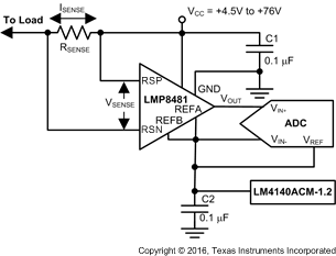
The LMP8480 and LMP8481 are precision high-side current sense amplifiers that amplify a small differential voltage developed across a current sense resistor in the presence of high input common-mode voltages. These amplifiers are designed for bidirectional (LMP8481) or unidirectional (LMP8480) current applications and accept input signals with common-mode voltage range from 4 V to 76 V with a bandwidth of 270 kHz. Because the operating power supply range overlaps the input common-mode voltage range, the LMP848x can be powered by the same voltage that is being monitored. This benefit eliminates the need for an intermediate supply voltage to be routed to the point of load where the current is being monitored, resulting in reduced component count and board space.
The LMP848x family consists of fixed gains of 20, 60, and 100 for applications that demand high accuracy over temperature. The low-input offset voltage allows the use of smaller sense resistors without sacrificing system error. The wide operating temperature range of –40°C to 125°C makes the LMP848x an ideal choice for automotive, telecommunications, industrial, and consumer applications. The LMP8480 and LMP8481 are pin-for-pin replacements for the MAX4080 and MAX4081, offering improved offset voltage, wider reference adjust range and higher output drive capabilities. The LMP8480 and LMP8481 are available in a 8-pin VSSOP package.
Device Information(1)
| PART NUMBER | PACKAGE | BODY SIZE (NOM) |
|---|---|---|
| LMP8480 | VSSOP (8) | 3.00 mm x 3.00 mm |
| LMP8481 | VSSOP (8) | 3.00 mm x 3.00 mm |
- For all available packages, see the orderable addendum at the end of the datasheet.
4 Revision History
Changes from D Revision (April 2016) to E Revision
- Deleted last Features bullet Go
- Deleted LMP8480-H row from Device Comparison TableGo
- Changed REFA to REFB and REFB to REFA for pins 6 and 7, respectively, in Pin Functions tableGo
- Deleted NCQ column from Thermal Information tableGo
- Changed bidirectional to unidirectional is description of Figure 22 in Basic Connections section Go
Changes from C Revision (September 2015) to D Revision
- Changed Typical Application Schematic: swapped RSN and RSP labelsGo
- Changed conditions of Electrical Characteristics table Go
- Added unit to ROUT parameter in Electrical Characteristics table Go
- Changed first paragraph of Overview section Go
Changes from B Revision (December 2014) to C Revision
- Deleted WSON package option for LMP8480 and LMP8481 Go
- Deleted -F version (50x gain) for LMP8480 and LMP8481Go
- Deleted WSON package options for LMP8480 and LMP8481 Go
Changes from A Revision (August 2012) to B Revision
- Added Pin Configuration and Functions section, ESD Ratings table, Feature Description section, Device Functional Modes, Application and Implementation section, Power Supply Recommendations section, Layout section, Device and Documentation Support section, and Mechanical, Packaging, and Orderable Information section Go
