SNVS311D May 2005 – February 2015 LP3878-ADJ
PRODUCTION DATA.
- 1 Features
- 2 Applications
- 3 Description
- 4 Revision History
- 5 Pin Configuration and Functions
- 6 Specifications
- 7 Detailed Description
- 8 Application and Implementation
- 9 Power Supply Recommendations
- 10Layout
- 11Device and Documentation Support
- 12Mechanical, Packaging, and Orderable Information
パッケージ・オプション
メカニカル・データ(パッケージ|ピン)
サーマルパッド・メカニカル・データ
発注情報
1 Features
- Input Supply Voltage: 2.5 V to 16V
- Output Voltage Range: 1 V to 5.5 V
- Designed for Use With Low-ESR Ceramic Capacitors
- Very Low Output Noise
- 8-Lead SO PowerPAD™ and WSON Surface-Mount Packages
- < 10-μA Quiescent Current in Shutdown
- Low Ground Pin Current at all Loads
- Overtemperature and Overcurrent Protection
- –40°C to 125°C Operating Junction Temperature Range
2 Applications
- ASIC Power Supplies In:
- Desktops, Notebooks, and Graphic Cards
- Set Top Boxes, Printers, and Copiers
- DSP and FPGA Power Supplies
- SMPS Post-Regulator
- Medical Instrumentation
3 Description
The LP3878-ADJ is an 800-mA, adjustable output, voltage regulator designed to provide high performance and low noise in applications requiring output voltages as low as 1 V.
Using an optimized VIP (Vertically Integrated PNP) process, the LP3878-ADJ delivers superior performance:
- Ground Pin Current: Typically 5.5 mA at 800-mA load, and 180 µA at 100-µA load.
- Low Power Shutdown: The LP3878-ADJ draws less than 10-μA quiescent current when the SHUTDOWN pin is pulled low.
- Precision Output: Ensured output voltage accuracy is 1% at room temperature.
- Low Noise: Broadband output noise is only 18 μV (typical) with a 10-nF bypass capacitor.
Device Information(1)
| PART NUMBER | PACKAGE | BODY SIZE (NOM) |
|---|---|---|
| LP3878-ADJ | SO PowerPAD (8) | 4.89 mm × 3.90 mm |
| WSON (8) | 4.00 mm × 4.00 mm |
- For all available packages, see the orderable addendum at the end of the data sheet.
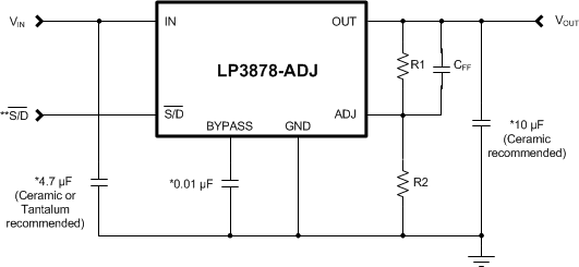
Basic Application Circuit

*Capacitor values shown are minimum required to assure stability. A larger output capacitor provides improved dynamic response. Output capacitor must meet ESR requirements (see Application Information).
**The SHUTDOWN (or S/D) pin must be actively terminated (see Device Functional Modes). Tie to IN (pin 4) if not used.
**The SHUTDOWN (or S/D) pin must be actively terminated (see Device Functional Modes). Tie to IN (pin 4) if not used.