SBOS688A April 2015 – October 2015 OPA2625 , OPA625
PRODUCTION DATA.
- 1 Features
- 2 Applications
- 3 Description
- 4 Revision History
- 5 Pin Configuration and Functions
-
6 Specifications
- 6.1 Absolute Maximum Ratings
- 6.2 ESD Ratings
- 6.3 Recommended Operating Conditions
- 6.4 Thermal Information
- 6.5 Electrical Characteristics High-Drive Mode
- 6.6 Electrical Characteristics Low-Power Mode
- 6.7 Electrical Characteristics High-Drive Mode
- 6.8 Electrical Characteristics Low-Power Mode
- 6.9 Switching Characteristics
- 6.10 Typical Characteristics
- 7 Parameter Measurement Information
- 8 Detailed Description
- 9 Application and Implementation
- 10Power Supply Recommendations
- 11Layout
- 12Device and Documentation Support
- 13Mechanical, Packaging, and Orderable Information
1 Features
- High-Drive Mode:
- GBW (G = 100): 120 MHz
- Slew Rate: 115 V/µs
- 16-Bit Settling at 4-V Step: 280 ns
- Low Voltage Noise: 2.5 nV/√Hz at 10 kHz
- Low Output Impedance: 1 Ω at 1 MHz
- Offset Voltage: ±100 µV (max)
- Offset Voltage Drift: ±3 µV/ºC (max)
- Low Quiescent Current: 2 mA (typ)
- Low-Power Mode:
- GBW: 1 MHz
- Low Quiescent Current: 270 µA (typ)
- Power-Scalable Features:
- Ultrafast Transition from Low-Power to High-Drive Mode: 170 ns
- High AC and DC Precision:
- Low Distortion: –122 dBc for HD2 and –140 dBc for HD3 at 100 kHz
- Input Common-Mode Range Includes Negative Rail
- Rail-to-Rail Output
- Wide Temperature Range: Fully Specified from –40°C to +125°C
2 Applications
- Precision SAR ADC Drivers
- Precision Voltage Reference Buffers
- Programmable Logic Controllers
- Test and Measurement Equipment
- Power-Sensitive Data Acquisition Systems
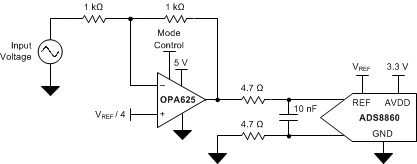
SAR ADC Driver

3 Description
The OPAx625 family of operational amplifiers are excellent 16-bit and 18-bit, high-precision, SAR ADC drivers with low THD and noise that allow for a unique power-scalable solution. This family of devices is fully characterized and specified with a 16-bit settling time of 280 ns that enables a true 16-bit effective number of bits (ENOB). With a high dc precision of only 100 µV offset voltage, a wide gain-bandwidth product of 120 MHz, and a low wideband noise of 2.5 nV/√Hz, this family is optimized for driving high-throughput, high-resolution SAR ADCs, such as the ADS88xx family of SAR ADCs.
The OPAx625 features two operating modes: high-drive and low-power. In the innovative low-power mode, the OPAx625 tracks the input signal allowing the device to transition from low-power mode to high-drive mode at 16-bit ENOB within 170 ns.
The OPAx625 family is available in 6-pin SOT and 10-pin VSSOP packages and is specified for operation from –40°C to +125°C.
Device Information(1)
| PART NUMBER | PACKAGE | BODY SIZE (NOM) |
|---|---|---|
| OPA625 | SOT (6) | 2.90 mm × 1.60 mm |
| OPA2625 | VSSOP (10) | 3.00 mm × 3.00 mm |
- For all available packages, see the package option addendum at the end of the data sheet.
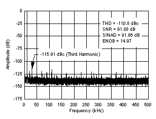
16-Bit SAR ADC, fIN = 10-kHz, 1-MSPS FFT
