SLOS432B April 2004 – October 2015 THS4281
PRODUCTION DATA.
- 1 Features
- 2 Applications
- 3 Description
- 4 Revision History
- 5 Pin Configuration and Functions
-
6 Specifications
- 6.1 Absolute Maximum Ratings
- 6.2 ESD Ratings
- 6.3 Recommended Operating Conditions
- 6.4 Thermal Information
- 6.5 Electrical Characteristics, VS = 3 V (VS+ = 3 V, VS- = GND)
- 6.6 Electrical Characteristics, VS = 5 V (VS+ = 5 V, VS- = GND)
- 6.7 Electrical Characteristics, VS = ±5 V
- 6.8 Dissipation Ratings
- 6.9 Typical Characteristics
- 7 Detailed Description
- 8 Application and Implementation
- 9 Power Supply Recommendations
- 10Layout
- 11Device and Documentation Support
- 12Mechanical, Packaging, and Orderable Information
パッケージ・オプション
デバイスごとのパッケージ図は、PDF版データシートをご参照ください。
メカニカル・データ(パッケージ|ピン)
- D|8
- DBV|5
- DGK|8
サーマルパッド・メカニカル・データ
発注情報
1 Features
- Very Low Quiescent Current: 750 μA (at 5 V)
- Rail-to-Rail Input and Output:
- Common-Mode Input Voltage Extends
400 mV Beyond the Rails - Output Swings Within 150 mV From the Rails
- Common-Mode Input Voltage Extends
- Wide –3-dB Bandwidth at 5 V:
- 90 MHz at Gain = +1, 40 MHz at Gain = +2
- High Slew Rate: 35 V/μs
- Fast Settling Time (2-V Step):
- 78 ns to 0.1%
- 150 ns to 0.01%
- Low Distortion at Gain = +2, VO = 2-VPP, 5 V:
- –91 dBc at 100 kHz, –67 dBc at 1 MHz
- Input Offset Voltage: 2.5 mV (Max at +25°C)
- Output Current > 30 mA (10-Ω Load, 5 V)
- Low Voltage Noise of 12.5 nV/√Hz
- Supply Voltages: +2.7 V, 3 V, +5 V, ±5 V, +15 V
- Packages: SOT23, MSOP, and SOIC
2 Applications
- Portable/Battery-Powered Applications
- High Channel Count Systems
- ADC Buffer
- Active Filters
- Current Sensing
3 Description
Fabricated using the BiCom-II process, the THS4281 is a low-power, rail-to-rail input and output, voltage-feedback operational amplifier designed to operate over a wide power-supply range of 2.7-V to 15-V single supply, and ±1.35-V to ±7.5-V dual supply. Consuming only 750 μA with a unity gain bandwidth of 90 MHz and a high 35-V/μs slew rate, the THS4281 allows portable or other power-sensitive applications to realize high performance with minimal power. To ensure long battery life in portable applications, the quiescent current is trimmed to be less than 900 μA at +25°C, and 1 mA from –40°C to +85°C.
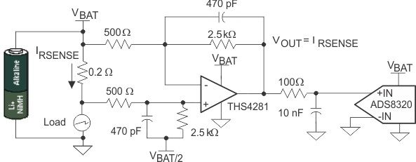
The THS4281 is a true single-supply amplifier with a specified common-mode input range of 400 mV beyond the rails. This allows for high-side current sensing applications without phase reversal concerns. Its output swings to within 40 mV from the rails with 10-kΩ loads, and 150 mV from the rails with 1-kΩ loads.
The THS4281 has a good 0.1% settling time of 78 ns, and 0.01% settling time of 150 ns. The low THD of –87 dBc at 100 kHz, coupled with a maximum offset voltage of less than 2.5 mV, makes the THS4281 a good match for high-resolution ADCs sampling less than 2 MSPS.
The THS4281 is offered in a space-saving SOT23-5 package, a small MSOP-8 package, and the industry standard SOIC-8 package.
Device Information(1)
| PART NUMBER | PACKAGE | BODY SIZE (NOM) |
|---|---|---|
| THS4281 | SOIC (8) | 4.90 mm × 3.91 mm |
| SOT-23 (5) | 2.90 mm × 1.60 mm | |
| VSSOP (8) | 3.00 mm × 3.00 mm |
- For all available packages, see the orderable addendum at the end of the data sheet.
High-side, Low Power Current-Sensing system
