SLASE75D August 2015 – September 2017 TMDS181
PRODUCTION DATA.
- 1 Features
- 2 Applications
- 3 Description
- 4 Revision History
- 5 Pin Configuration and Functions
-
6 Specifications
- 6.1 Absolute Maximum Ratings
- 6.2 ESD Ratings
- 6.3 Recommended Operating Conditions
- 6.4 Thermal Information
- 6.5 Power Supply Electrical Characteristics
- 6.6 TMDS Differential Input Electrical Characteristics
- 6.7 TMDS Differential Output Electrical Characteristics
- 6.8 DDC, I2C, HPD, and ARC Electrical Characteristics
- 6.9 Power-Up and Operation Timing Requirements
- 6.10 TMDS Switching Characteristics
- 6.11 HPD Switching Characteristics
- 6.12 DDC and I2C Switching Characteristics
- 6.13 Typical Characteristics
- 7 Parameter Measurement Information
-
8 Detailed Description
- 8.1 Overview
- 8.2 Functional Block Diagram
- 8.3
Feature Description
- 8.3.1 Reset Implementation
- 8.3.2 Operation Timing
- 8.3.3 Swap and Polarity Working
- 8.3.4 TMDS Inputs
- 8.3.5 TMDS Inputs Debug Tools
- 8.3.6 Receiver Equalizer
- 8.3.7 Input Signal Detect Block
- 8.3.8 Audio Return Channel
- 8.3.9 Transmitter Impedance Control
- 8.3.10 TMDS Outputs
- 8.3.11 Pre-Emphasis/De-Emphasis
- 8.4 Device Functional Modes
- 8.5 Register Maps
- 9 Application and Implementation
- 10Power Supply Recommendations
- 11Layout
- 12Device and Documentation Support
- 13Mechanical, Packaging, and Orderable Information
パッケージ・オプション
メカニカル・データ(パッケージ|ピン)
- RGZ|48
サーマルパッド・メカニカル・データ
- RGZ|48
発注情報
1 Features
- HDMI™ Input Port to Output Port With CDR Supporting Up to 6 Gbps Data Rates
- Compatible With HDMI™ Electrical Parameters Up to 6 Gbps in Retimer Mode
- Support 4k2k60p and Up to WUXGA 16-Bit Color Depth or 1080p With Higher Refresh Rates
- Retimes Input Stream to Compensate for Random Jitter
- Adaptive Receiver Equalizer or Programmable Fixed Equalizer
- I2C and Pin Strap Programmable
- Inter-Pair Skew Compensation of 5+ Bits
- Single-Ended Mode ARC Support
- Link Debug Tools Including Eye Diagram After the RX Equalizer
- 48-Pin 7-mm × 7-mm 0.5-mm Pitch VQFN Package
- Extended Commercial Temperature Support 0°C to 85°C (TMDS181)
- Industrial Temperature Support: –40°C to 85°C (TMDS181I)
2 Applications
- Digital TV
- Digital Projector
- Audio/Video Equipment
- Blu-ray™ DVD
- Monitors
- Desktops/ All-in-Ones
- Active Cables
3 Description
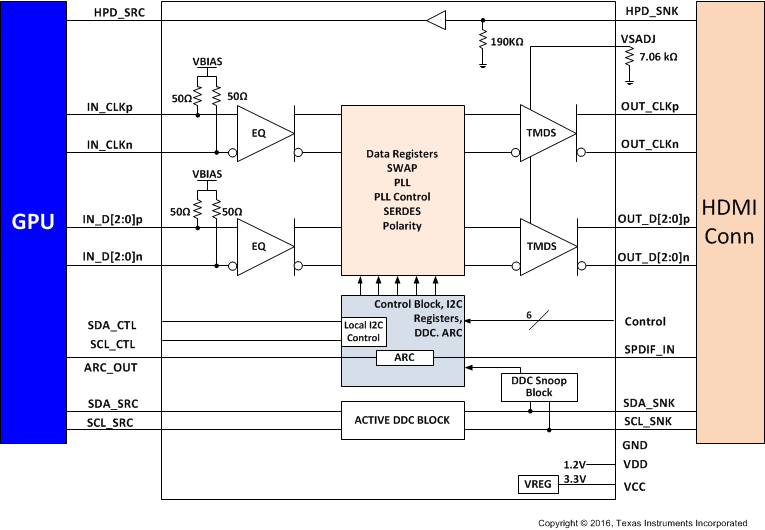
The TMDS181x is a digital video interface (DVI) or high-definition multimedia interface (HDMI™) retimer. The TMDS181x supports four TMDS channels, audio return channel (SPDIF_IN/ARC_OUT), and digital display control (DDC) interfaces. The TMDS181x supports signaling rates up to 6 Gbps to allow for the highest resolutions of 4k2k60p 24 bits per pixel and up to WUXGA 16-bit color depth or 1080p with higher refresh rates. The TMDS181x can be configured to support the HDMI2.0a standard. The TMDS181x automatically configures itself as a redriver at low data rate (<1.0 Gbps) or as a retimer above this data rate. Redriver mode supports HDMI1.4b with data rates up to 3.4 Gbps
The TMDS181x supports dual power supply rails of 1.2 V on VDD and 3.3 V on VCC for power reduction. Several methods of power management are implemented to reduce overall power consumption. TMDS181x supports fixed receive EQ gain or adaptive receive EQ control by I2C or pin strap to compensate for different lengths input cable or board traces.
Device Information(1)
| PART NUMBER | PACKAGE | BODY SIZE (NOM) |
|---|---|---|
| TMDS181 | VQFN (48) | 7.00 mm × 7.00 mm |
| TMDS181I |
- For all available packages, see the orderable addendum at the end of the data sheet.
SPACE
Simplified Schematic

