SLVSDG8B April 2016 – June 2017 TPS25740 , TPS25740A
PRODUCTION DATA.
- 1 Features
- 2 Applications
- 3 Description
- 4 Revision History
- 5 Device Comparison Table
- 6 Pin Configuration and Functions
- 7 Specifications
-
8 Detailed Description
- 8.1 Overview
- 8.2 Functional Block Diagram
- 8.3
Feature Description
- 8.3.1 USB Type-C CC Logic (CC1, CC2)
- 8.3.2 USB PD BMC Transmission (CC1, CC2, VTX)
- 8.3.3 USB PD BMC Reception (CC1, CC2)
- 8.3.4 Discharging (DSCG, VPWR)
- 8.3.5 Configuring Voltage Capabilities (HIPWR, EN9V, EN12V)
- 8.3.6 Configuring Power Capabilities (PSEL, PCTRL, HIPWR)
- 8.3.7 Gate Driver (GDNG, GDNS)
- 8.3.8 Fault Monitoring and Protection
- 8.3.9 Voltage Control (CTL1, CTL2)
- 8.3.10 Sink Attachment Indicator (UFP, DVDD)
- 8.3.11 Power Supplies (VAUX, VDD, VPWR, DVDD)
- 8.3.12 Grounds (AGND, GND)
- 8.3.13 Output Power Supply (DVDD)
- 8.4 Device Functional Modes
-
9 Application and Implementation
- 9.1
Application Information
- 9.1.1 System-Level ESD Protection
- 9.1.2 Use of GD Internal Clamp
- 9.1.3 Resistor Divider on GD for Programmable Start Up
- 9.1.4 Selection of the CTL1 and CTL2 Resistors (R(FBL1) and R(FBL2))
- 9.1.5 Voltage Transition Requirements
- 9.1.6 VBUS Slew Control using GDNG C(SLEW)
- 9.1.7 Tuning OCP Using RF and CF
- 9.2 Typical Application , A/C Power Source (Wall Adapter)
- 9.3 System Examples
- 9.1
Application Information
- 10Power Supply Recommendations
- 11Layout
- 12Device and Documentation Support
- 13Mechanical, Packaging, and Orderable Information
パッケージ・オプション
メカニカル・データ(パッケージ|ピン)
- RGE|24
サーマルパッド・メカニカル・データ
- RGE|24
発注情報
1 Features
- USB Power Delivery (PD) 2.0 Certified Provider,
USB Type-C™ Rev. 1.2 Compliant Source - Pin-Selectable Voltage Advertisement
- 5 V, 12 V, and/or 20 V (TPS25740)
- 5 V, 9 V, and/or 15 V (TPS25740A)
- Pin-Selectable Peak Power Settings
- 12 options 15 W – 100W (TPS25740)
- 11 options 15 W – 81W (TPS25740A)
- High Voltage and Safety Integration
- Overvoltage, Overcurrent, Overtemperature Protection and VBUS Discharge
- IEC 61000-4-2 Protection on CC1 and CC2
- Input Pin for Fast Shutdown Under Fault
- Control of External N-ch MOSFET
- 2-pin External Power Supply Control
- Wide VIN Supply (4.65 V – 25 V)
- Below 10 µA Quiescent Current when Unattached
- Port Attachment Indicator
- Port Power Management
- Built-In 1.8 V at 35 mA Supply Output
2 Applications
- USB-PD Adaptor (data-less)
- Dedicated Charging Port (data-less)
- Power Hub (data-less)
- Power Bank
- Cigarette Lighter Adaptor (CLA)
3 Description
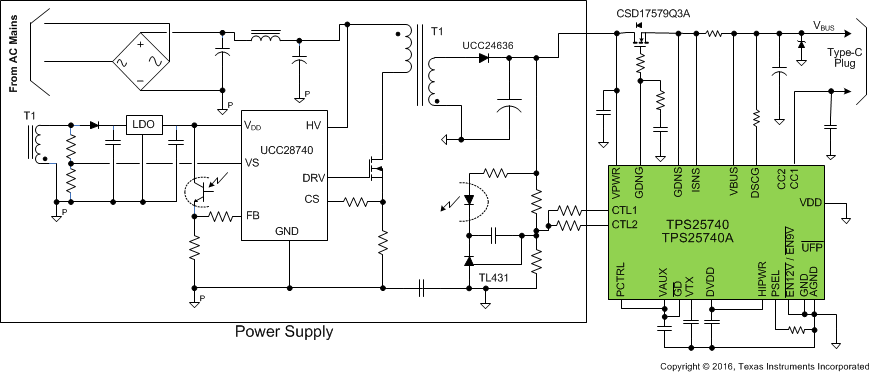
The TPS25740, TPS25740A implements a source that is compliant to USB Power Delivery 2.0 version 1.2 and Type-C revision 1.2. It monitors the CC pin to detect when a USB Type-C sink is attached, then it enables a N-ch MOSFET gate driver to turn on VBUS. The device then offers up to three different voltages using USB Power Delivery. Four input pins (PSEL, HIPWR, PCTRL, and (EN12V or EN9V) are used to configure the voltages and currents advertised. The device uses the CTL1 and CTL2 pins to select one of three voltages from the power supply based on the voltage requested by the attached sink. The device automatically handles discharging the VBUS output per USB PD requirements.
The TPS25740, TPS25740A typically draws 8.5 µA (or 5.8 µA if VDD = 3.3 V) when no device is attached. Additional system power saving is achievable by using the Port Attachment Indicator (UFP) output to disable the power source when no device is attached.
Protection features include overvoltage protection, overcurrent protection, over-temperature protection, IEC for CC pins, and system override to disable the gate driver (GD).
Device Information(1)
| PART NUMBER | PACKAGE | BODY SIZE (NOM) |
|---|---|---|
| TPS25740 | QFN (24) | 4.00 mm x 4.00 mm |
| TPS25740A |
- For all available packages, see the orderable addendum at the end of the data sheet.
Simplified Schematic
