SLVSCV0B August 2015 – September 2016
PRODUCTION DATA.
- 1 Features
- 2 Applications
- 3 Description
- 4 Revision History
- 5 Device Comparison Table
- 6 Pin Configuration and Functions
- 7 Specifications
- 8 Detailed Description
-
9 Application and Implementation
- 9.1 Application Information
- 9.2
Typical Applications
- 9.2.1
Simple 3.7-A eFuse Protection for Set Top Boxes
- 9.2.1.1 Design Requirements
- 9.2.1.2 Detailed Design Procedure
- 9.2.1.3 Application Curves
- 9.2.2 Inrush and Reverse Current Protection for Hold-Up Capacitor Application (for example, SSD)
- 9.2.3 Controlled Power Down using TPS25923x
- 9.2.1
Simple 3.7-A eFuse Protection for Set Top Boxes
- 10Power Supply Recommendations
- 11Layout
- 12Device and Documentation Support
- 13Mechanical, Packaging, and Orderable Information
パッケージ・オプション
メカニカル・データ(パッケージ|ピン)
- DRC|10
サーマルパッド・メカニカル・データ
- DRC|10
発注情報
1 Features
- 5-V eFuse, VABSMAX = 20 V
- Integrated 28-mΩ Pass MOSFET
- Fixed 6.1-V Over Voltage Clamp
- 1-A to 5-A Adjustable ILIMIT
- ±8% ILIMIT Accuracy at 3.7A
- Reverse Current Blocking Support
- Programmable OUT Slew Rate, UVLO
- Built-in Thermal Shutdown
- UL 2367 Recognized – File No. E339631*
- *RILIM ≤ 130 kΩ (5 A maximum)
- Safe During Single Point Failure Test (UL60950)
- Small Foot Print – 10L (3 mm x 3 mm) VSON
2 Applications
- Adapter Powered Devices
- HDD and SSD Drives
- Set Top Boxes
- Servers / AUX Supplies
- Fan Control
- PCI/PCIe Cards
3 Description
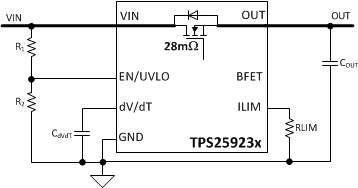
The TPS25923x family of eFuses is a highly integrated circuit protection and power management solution in a tiny package. The devices use few external components and provide multiple protection modes. They are a robust defense against overloads, shorts circuits, voltage surges, excessive inrush current, and reverse current.
Current limit level can be set with a single external resistor. Over voltage events are limited by internal clamping circuits to a safe fixed maximum, with no external components required. Applications with particular voltage ramp requirements can set dV/dT with a single capacitor to ensure proper output ramp rates.
Many systems, such as SSDs, must not allow holdup capacitance energy to dump back through the FET body diode onto a drooping or shorted input bus. The BFET pin is for such systems. An external NFET can be connected “Back to Back (B2B)” with the TPS25923x output and the gate driven by BFET to prevent current flow from load to source (see Figure 43).
Device Information(1)
| PART NUMBER | PACKAGE | BODY SIZE (NOM) |
|---|---|---|
| TPS259230 | VSON (10) | 3.00 mm × 3.00 mm |
| TPS259231 |
- For all available packages, see the orderable addendum at the end of the data sheet.
Application Schematic

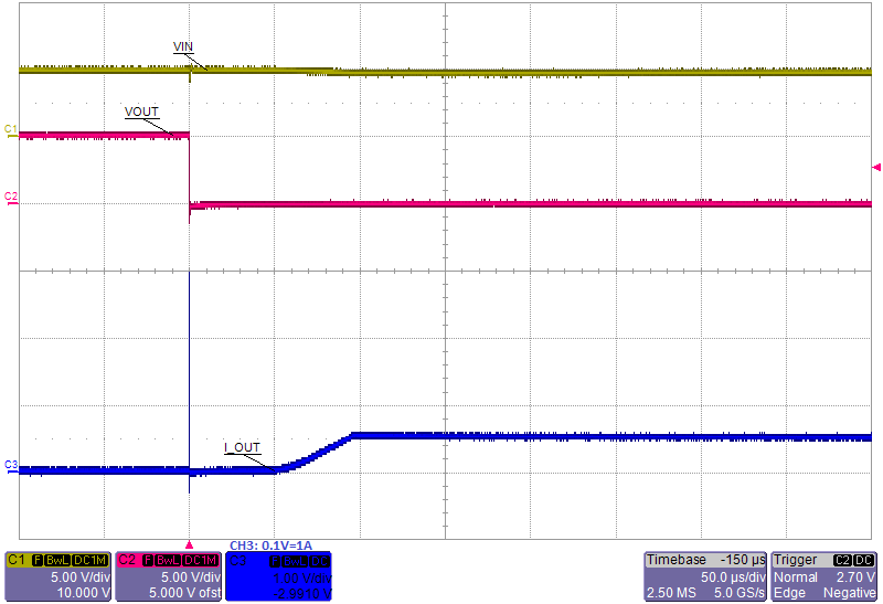
Transient: Output Short Circuit
