SBVS228B July 2013 – March 2015 TPS7A3501
PRODUCTION DATA.
- 1 Features
- 2 Applications
- 3 Description
- 4 Revision History
- 5 Pin Configuration and Functions
- 6 Specifications
- 7 Detailed Description
- 8 Application and Implementation
- 9 Power Supply Recommendations
- 10Layout
- 11Device and Documentation Support
- 12Mechanical, Packaging, and Orderable Information
パッケージ・オプション
メカニカル・データ(パッケージ|ピン)
- DRV|6
サーマルパッド・メカニカル・データ
- DRV|6
発注情報
1 Features
- Regulates Input-to-Output Voltage:
-
Power-Supply Rejection Ratio:
- 42 dB at 1 MHz
- ≥ 32 dB (360 kHz to 3.9 MHz)
- Low-Noise Output:
- 3.8 µVRMS (10 Hz to 100 kHz)
- Output Current: Up to 1 A
- Output Voltage Range: 1.21 V to 4.5 V
- Excellent Load Transient Response
- Stable With Ceramic Capacitors as Low as
10 µF - Current Limit and Thermal Shutdown for
Fault Protection - Available in a Low Thermal Resistance Package: 2-mm × 2-mm WSON-6
- Operating Temperature Range:
–40°C to 125°C
2 Applications
3 Description
The TPS7A3501 is a positive voltage, low-noise
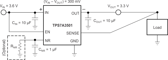
(3.8-µVRMS) power filter capable of sourcing a 1-A load suitable for quiet supply solutions. Power filters, such as the TPS7A3501, provide voltage regulation across the input and output terminals with high efficiency (low insertion loss), and power-supply rejection. The device is ideally suited as a noise filter for 3.3-V, 2.5-V, and 1.8-V supplies at up to 1 A.
The input-to-output voltage regulation is also user-programmable, from 200 mV to 500 mV, with a single external resistor. If no resistor is used, the TPS7A3501 provides 330 mV of input-to-output voltage regulation. The device is stable with 10-µF input and output ceramic capacitors and a 10-nF noise-reduction ceramic capacitor.
The TPS7A3501 is fully specified over a wide temperature of –40°C to 125°C. The device is offered in a low thermal resistance, 2-mm × 2-mm, WSON-6 package. Unlike passive filters, the TPS7A3501 provides thermal and current protection for itself and surrounding circuitry.
Device Information(1)
| PART NUMBER | PACKAGE | BODY SIZE (NOM) |
|---|---|---|
| TPS7A3501 | WSON (6) | 2.00 mm × 2.00 mm |
- For all available packages, see the orderable addendum at the end of the data sheet.
