SLUSA87C August 2010 – October 2015 UCC24610
PRODUCTION DATA.
- 1 Features
- 2 Applications
- 3 Description
- 4 Revision History
- 5 Pin Configuration and Functions
- 6 Specifications
- 7 Detailed Description
-
8 Application and Implementation
- 8.1 Application Information
- 8.2
Typical Application
- 8.2.1 Design Requirements
- 8.2.2 Detailed Design Procedure
- 8.2.3 Application Curves
- 9 Power Supply Recommendations
- 10Layout
- 11Device and Documentation Support
- 12Mechanical, Packaging, and Orderable Information
パッケージ・オプション
メカニカル・データ(パッケージ|ピン)
サーマルパッド・メカニカル・データ
- DRB|8
発注情報
1 Features
- Secondary-Side Controller Optimized for 5-V Systems
- Up to 600-kHz Operating Frequency
- VDS MOSFET-Sensing
- 1.6-Ω Sink, 2.0-Ω Source Gate-Drive Impedances
- Micro-Power Sleep Current for 90+ Designs
- Automatic Light-Load Management
- Synchronous Wake-Up From Sleep and Light-Load Modes
- Protection Features on Programming Inputs
- SYNC Input for CCM Operation
- 20-ns Typical Turnoff Propagation Delay
- Improved Efficiency and Design Flexibility Over Traditional Diode Solution
- May Be Biased Directly From 5-V Output
- Minimal Component Count
2 Applications
- AC-to-DC 5-V Adapters
- 5-V Bias Supplies
- Low Voltage Rectification Circuits
- Flyback and LLC Converters
3 Description
This GREEN Rectifier™ controller is a high-performance controller and driver for standard and logic-level N-channel MOSFET power devices used for low-voltage secondary-side synchronous rectification.
The combination of controller and MOSFET emulates a near-ideal diode rectifier. This solution not only directly reduces power dissipation of the rectifier but also indirectly reduces primary-side losses as well, due to compounding of efficiency gains.
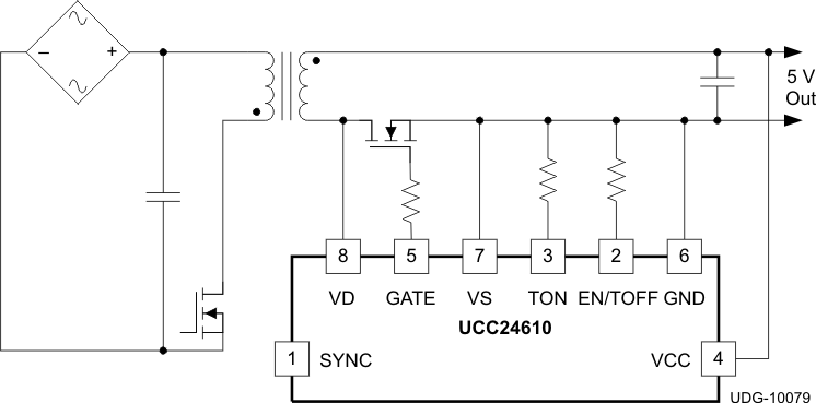
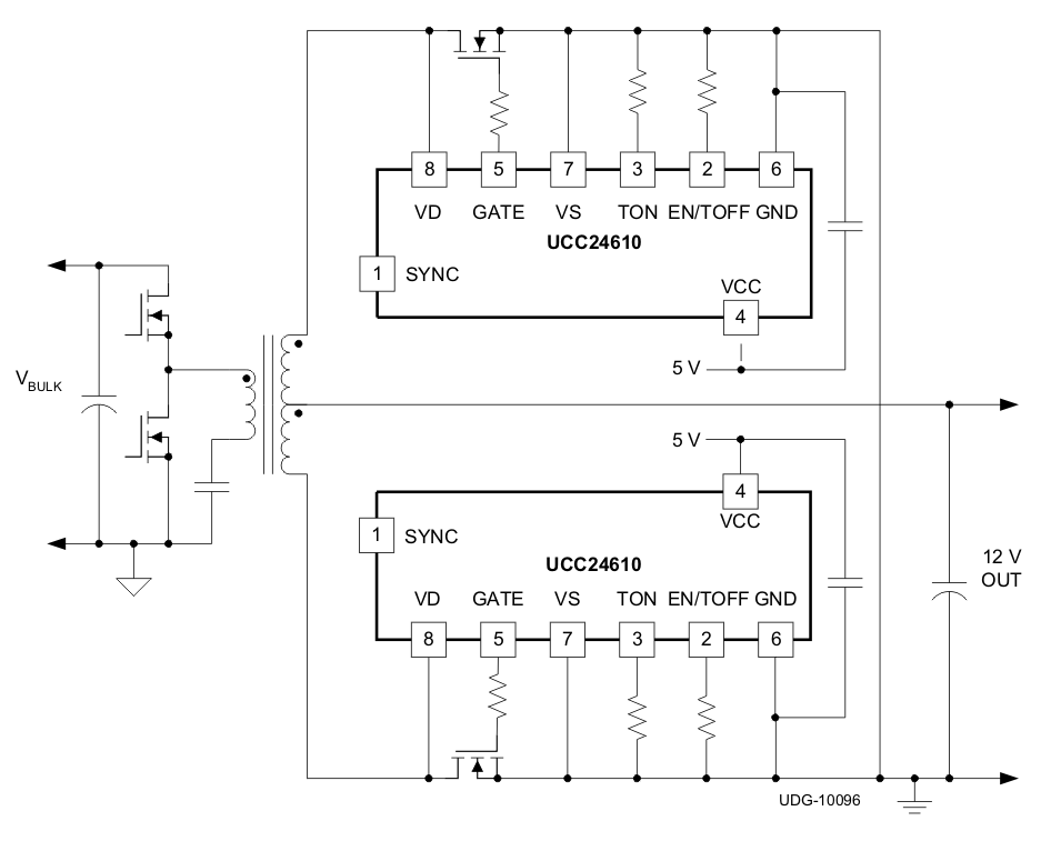
Using drain-to-source voltage sensing, the UCC24610 is ideal for Flyback and LLC-resonant power supplies but can also be used with other power architectures. The UCC24610 is optimized for output voltages from 4.5 V to 5.5 V, and is suitable for use with lower and higher output voltages as well.
The UCC24610 offers a programmable false-triggering filter, a programmable timer to automatically switch to light-load mode at light load, and a SYNC input for optional use in continuous conduction mode (CCM) systems. Protection features on TON and EN/TOFF pins prevent run-away on-time due to open-circuit or short-circuit fault conditions.
This device is available in an 8-pin SOIC package and an 8-pin, 3.0-mm × 3.0-mm SON package with an exposed thermal pad.
Device Information(1)
| PART NUMBER | PACKAGE | BODY SIZE (NOM) |
|---|---|---|
| UCC24610DRB | SON (8) | 3.00 mm × 3.00 mm |
| UCC24610D | SOIC (8) | 4.90 mm × 3.91 mm |
- For all available packages, see the orderable addendum at the end of the data sheet.
Flyback Topology

LLC-Resonant Half Bridge
