SGLS387H July 2007 – August 2016 DAC5675A-SP
PRODUCTION DATA.
- 1 Features
- 2 Applications
- 3 Description
- 4 Revision History
- 5 Description (continued)
- 6 Pin Configuration and Functions
-
7 Specifications
- 7.1 Absolute Maximum Ratings
- 7.2 ESD Ratings
- 7.3 Recommended Operating Conditions
- 7.4 Thermal Information
- 7.5 DC Electrical Characteristics (Unchanged After 100 kRad)
- 7.6 AC Electrical Characteristics (Unchanged After 100 kRad)
- 7.7 Digital Specifications (Unchanged After 100 kRad)
- 7.8 Electrical Characteristics
- 7.9 Typical Characteristics
- 8 Detailed Description
- 9 Application and Implementation
- 10Power Supply Recommendations
- 11Layout
- 12Device and Documentation Support
- 13Mechanical, Packaging, and Orderable Information
パッケージ・オプション
デバイスごとのパッケージ図は、PDF版データシートをご参照ください。
メカニカル・データ(パッケージ|ピン)
- HFG|52
サーマルパッド・メカニカル・データ
発注情報
1 Features
- QMLV (QML Class V) MIL-PRF-38535 Qualified, SMD 5962-07204
- 5962-0720401VXC – Qualified over the Military Temperature Range (–55°C to 125°C)
- 5962-0720402VXC – Qualified over Reduced Temperature Range (–55°C to 115°C) for Improved Dynamic Performance
- High-Performance 52-Pin Ceramic Quad Flat Pack (HFG)
- 400-MSPS Update Rate
- LVDS-Compatible Input Interface
- Spurious-Free Dynamic Range (SFDR) to Nyquist
- 69 dBc at 70 MHz IF, 400 MSPS
- W-CDMA Adjacent Channel Power Ratio (ACPR)
- 73 dBc at 30.72 MHz IF, 122.88 MSPS
- 71 dBc at 61.44 MHz IF, 245.76 MSPS
- Differential Scalable Current Outputs: 2 to 20 mA
- On-Chip 1.2-V Reference
- Single 3.3-V Supply Operation
- Power Dissipation: 660 mW at ƒCLK = 400 MSPS, ƒOUT = 20 MHz
2 Applications
- Radiation Hardened Digital to Analog (DAC) Applications
- Space Satellite RF Data Transmission
- Cellular Base Transceiver Station Transmit Channel:
- CDMA: WCDMA, CDMA2000, IS-95
- TDMA: GSM, IS-136, EDGE/GPRS
- Supports Single-Carrier and Multicarrier Applications
- Engineering Evaluation (/EM) Samples are Available (1)
3 Description
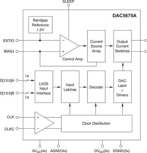
The DAC5675A-SP is a radiation-tolerant, 14-bit resolution high-speed digital-to-analog converter (DAC) primarily suited for space satellite applications. The DAC5675A-SP is designed for high-speed digital data transmission in wired and wireless communication systems, high-frequency direct digital synthesis (DDS), and waveform reconstruction in test and measurement applications. The DAC5675A-SP has excellent SFDR at high intermediate frequencies, which makes it well suited for multicarrier transmission in TDMA and CDMA based cellular base transceiver stations (BTSs).
The DAC5675A-SP operates from a single supply voltage of 3.3 V. Power dissipation is 660 mW at ƒCLK = 400 MSPS, ƒOUT = 70 MHz. The DAC5675A-SP provides a nominal full-scale differential current output of 20 mA, supporting both single-ended and differential applications. The output current can be directly fed to the load with no additional external output buffer required. The output is referred to the analog supply voltage AVDD.
The DAC5675A-SP includes a low-voltage differential signaling (LVDS) interface for high-speed digital data input. LVDS features a low differential voltage swing with a low constant power consumption across frequency, allowing for high-speed data transmission with low noise levels (low electromagnetic interference (EMI)).
Device Information(1)
| PART NUMBER | PACKAGE | BODY SIZE (NOM) |
|---|---|---|
| DAC5675A-SP | HFG (52 CQFP) | 19.05 mm × 19.05 mm |
- For all available packages, see the orderable addendum at the end of the data sheet.
Simplified Schematic

4 Revision History
Changes from G Revision (August 2014) to H Revision
- Updated supply voltage absolute maximum rating for AVDD to DVDD Go
- Added sentence explaining AVDD and DVDD simultaneous rampGo
- Added Receiving Notification of Documentation Updates and Community Resources sectionsGo
Changes from F Revision (January 2014) to G Revision
- Added ESD Ratings table, Feature Description section, Device Functional Modes, Application and Implementation section, Power Supply Recommendations section, Layout section, Device and Documentation Support section, and Mechanical, Packaging, and Orderable Information section Go
- Updated supply voltage absolute maximum ratings for AVDD to DVDD Go
Changes from E Revision (April 2013) to F Revision