SLAS767B June 2011 – March 2015 DAC7551-Q1
PRODUCTION DATA.
- 1 Features
- 2 Applications
- 3 Description
- 4 Revision History
- 5 Pin Configuration and Functions
- 6 Specifications
- 7 Detailed Description
- 8 Application and Implementation
- 9 Power Supply Recommendations
- 10Layout
- 11Device and Documentation Support
- 12Mechanical, Packaging, and Orderable Information
1 Features
- Qualified for Automotive Applications
- Relative Accuracy (INL): ±0.35 LSB
- Ultra-Low Glitch Energy: 0.1 nV-s
- Low-Power Operation: 100 μA at 2.7 V
- Power-On Reset-to-Zero Scale
- Power Supply: 2.7- to 5.5-V Single Supply
- Power-Down: 0.05 μA at 2.7 V
- 12-Bit Linearity and Monotonicity
- Rail-to-Rail Voltage Output
- Settling Time: 5 μs (Max)
- SPI-Compatible Serial Interface With Schmitt-Trigger Input: Up to 50 MHz
- Daisy-Chain Capability
- Asynchronous Hardware Clear-to-Zero Scale
- Specified Temperature Range:
–40°C to +105°C - Small, 2-mm × 3-mm, 12-Lead USON Package
- Z-Suffix Offers Improved Delamination
2 Applications
3 Description
The DAC7551-Q1 device is a single-channel, voltage-output digital-to-analog converter (DAC) with exceptional linearity and monotonicity, and a proprietary architecture that minimizes glitch energy. The low-power DAC7551-Q1 device operates from a single 2.7- to 5.5-V supply. The DAC7551-Q1 output amplifiers can drive a 2-kΩ, 200-pF load rail-to-rail with 5-μs settling time. The output range is set using an external voltage reference.
The 3-wire serial interface operates at clock rates up to 50 MHz and is compatible with SPI™, QSPI™, microwire, and DSP interface standards. The device incorporates a power-on-reset (POR) circuit to ensure that the DAC output powers up to 0 V and remains at that voltage until a valid write cycle to the device occurs. The device contains a power-down feature that reduces the current consumption of the device to under 2 μA.
Small size and low-power operation make the DAC7551-Q1 device ideally suited for battery-operated, portable applications. The power consumption is typically 0.5 mW at 5 V, 0.23 mW at
3 V, and reduces to 1 μW in power-down mode.
The DAC7551-Q1 device is available in a 12-pin USON package and is specified over –40°C to +105°C. The Z-suffix offers reduced delamination compared to standard device.
Device Information(1)
| PART NUMBER | PACKAGE | BODY SIZE (NOM) |
|---|---|---|
| DAC7551-Q1 | USON (12) | 2.00 mm × 3.00 mm |
- For all available packages, see the orderable addendum at the end of the data sheet.
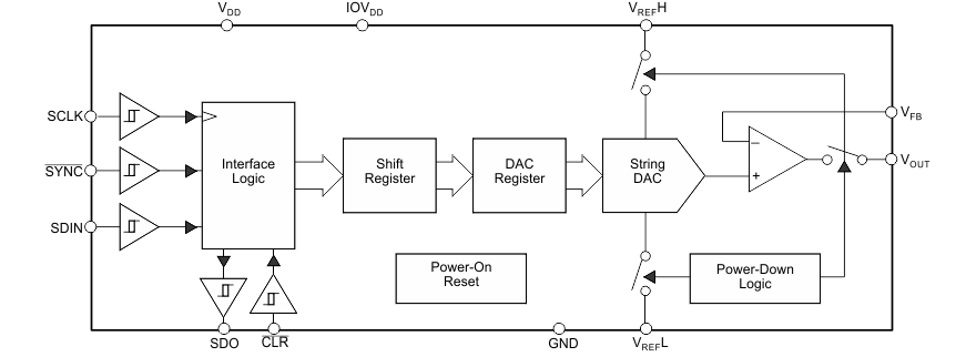
Functional Block Diagram
