SLUS888G JANUARY 2009 – September 2015
PRODUCTION DATA.
- 1 Features
- 2 Applications
- 3 Description
- 4 Revision History
- 5 Pin Configuration and Functions
- 6 Specifications
- 7 Detailed Description
- 8 Application and Implementation
- 9 Power Supply Recommendations
- 10Layout
- 11Device and Documentation Support
- 12Mechanical, Packaging, and Orderable Information
1 Features
- Cascoded Configuration Allows Fully Integrated Current Control Without External Sense Resistor
- Fast Start Up With Low Standby Power Achieved by Cascode Configuration
- Frequency and Peak Current Modulation for Optimum Efficiency Over Entire Operating Range
- Green-Mode (GM) Burst Switching Packets Improve No-Load Efficiency
- Advanced Overcurrent Protection Limits RMS Input and Output Currents
- Thermal Shutdown
- Timed Overload With Retry or Latch-Off Response
- Programmable Opto-Less Output Overvoltage Protection
- Fast Latched Fault Recovery
- 8-Pin SOIC Package and 8-Pin PDIP Lead-Free Packages
2 Applications
- Universal Input AC and DC Adapters, 12 to 65 W
- High Efficiency Housekeeping and Auxillary Power Supplies
- Offline Battery Chargers
- Consumer Electronics (DVD Players, Set-Top Boxes, DTV, Gaming, Printers)
3 Description
The UCC28610 brings a new level of performance and reliability to the AC and DC consumer power supply solution.
A PWM modulation algorithm varies both the switching frequency and primary current while maintaining discontinuous or transition mode operation over the entire operating range. Combined with a cascoded architecture, these innovations result in efficiency, reliability, and system cost improvements over a conventional flyback architecture.
The UCC28610 offers a predictable maximum power threshold and a timed response to an overload, allowing safe handling of surge power requirements. Overload fault response is user-programmed for retry or latch-off mode. Additional protection features include output overvoltage detection, programmable maximum on-time, and thermal shutdown.
Device Information(1)
| PART NUMBER | PACKAGE | BODY SIZE (NOM) |
|---|---|---|
| UCC28610 | SOIC (8) | 4.90 mm x 3.91 mm |
| PDIP (8) | 9.81 mm x 6.35 mm |
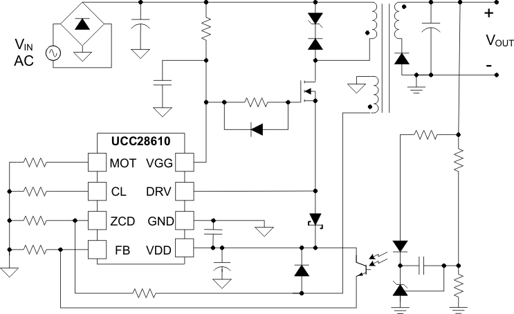
Simplified Application Schematic
