SNOS738I April 1995 – January 2017 LM9061 , LM9061-Q1
PRODUCTION DATA.
- 1 Features
- 2 Applications
- 3 Description
- 4 Revision History
- 5 Pin Configuration and Functions
- 6 Specifications
- 7 Detailed Description
- 8 Application and Implementation
- 9 Power Supply Recommendations
- 10Layout
- 11Device and Documentation Support
- 12Mechanical, Packaging, and Orderable Information
1 Features
- Qualified for Automotive Applications
- AEC-Q100 Qualified With the Following Results:
- Device HBM ESD Classification Level 2
- Device CDM ESD Classification Level C4B
- Withstands 60-V Supply Transients
- Overvoltage Shut-OFF With VCC > 30 V
- Lossless Overcurrent Protection Latch-OFF
- Current Sense Resistor is Not Required
- Minimizes Power Loss With High Current Loads
- Programmable Delay of Protection Latch-OFF
- Gradual Turnoff to Minimize Inductive Load Transient Voltages
- CMOS Logic-Compatible ON and OFF Control Input
2 Applications
- Transmission Control Units (TCU)
- Engine Control Units (ECU)
- Valve, Relay, and Solenoid Drivers
- Lamp Drivers
- DC Motor PWM Drivers
- Logic-Controlled Power Supply Distribution Switches
- Electronic Circuit Breakers
- High-Power Audio Speakers
3 Description
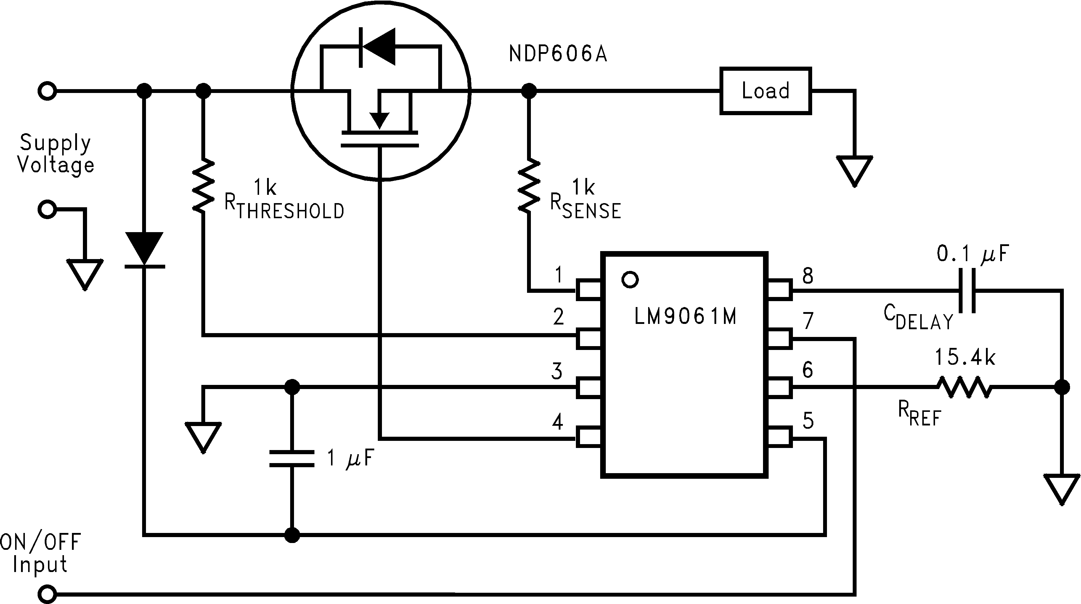
The LM9061 family consists of charge-pump devices which provides the gate drive to an external power MOSFET of any size configured as a high-side driver or switch. This includes multiple parallel connected MOSFETs for very high current applications. A CMOS logic-compatible ON and OFF input controls the output gate drive voltage. In the ON state, the charge pump voltage, which is well above the available VCC supply, is directly applied to the gate of the MOSFET. A built-in 15-V Zener clamps the maximum gate to source voltage of the MOSFET. When commanded OFF a 110-µA current sink discharges the gate capacitances of the MOSFET for a gradual turnoff characteristic to minimize the duration of inductive load transient voltages and further protect the power MOSFET.
Lossless protection of the power MOSFET is a key feature of the LM9061. The voltage drop (VDS) across the power device is continually monitored and compared against an externally programmable threshold voltage. A small current-sensing resistor in series with the load, which causes a loss of available energy, is not required for the protection circuitry. If the VDS voltage, due to excessive load current, exceeds the threshold voltage, the output is latched OFF in a more gradual fashion (through a 10-µA output current sink) after a programmable delay time interval.
Device Information(1)
| PART NUMBER | PACKAGE | BODY SIZE (NOM) |
|---|---|---|
| LM9061, LM9061-Q1 | SOIC (8) | 4.9 mm × 3.91 mm |
- For all available packages, see the orderable addendum at the end of the data sheet.
High-Side Driving and Protection to a Connected Load
