SNVSA81A February 2015 – April 2015 LMR14030
PRODUCTION DATA.
- 1 Features
- 2 Applications
- 3 Description
- 4 Simplified Schematic
- 5 Revision History
- 6 Pin Configuration and Functions
- 7 Specifications
-
8 Detailed Description
- 8.1 Overview
- 8.2 Functional Block Diagram
- 8.3
Feature Description
- 8.3.1 Fixed Frequency Peak Current Mode Control
- 8.3.2 Slope Compensation
- 8.3.3 Sleep-mode
- 8.3.4 Low Dropout Operation and Bootstrap Voltage (BOOT)
- 8.3.5 Adjustable Output Voltage
- 8.3.6 Enable and Adjustable Under-voltage Lockout
- 8.3.7 External Soft-start
- 8.3.8 Switching Frequency and Synchronization (RT/SYNC)
- 8.3.9 Over Current and Short Circuit Protection
- 8.3.10 Overvoltage Protection
- 8.3.11 Thermal Shutdown
- 9 Application and Implementation
- 10Power Supply Recommendations
- 11Layout
- 12Device and Documentation Support
- 13Mechanical, Packaging, and Orderable Information
パッケージ・オプション
メカニカル・データ(パッケージ|ピン)
- DDA|8
サーマルパッド・メカニカル・データ
- DDA|8
発注情報
1 Features
- 4 V to 40 V Input Range
- 3.5 A Continuous Output Current
- Ultra-low 40 µA Operating Quiescent Current
- 90 mΩ High-Side MOSFET
- Minimum Switch-On Time: 75 ns
- Current Mode Control
- Adjustable Switching Frequency from 200 kHz to 2.5 MHz
- Frequency Synchronization to External Clock
- Internal Compensation for Ease of Use
- High Duty Cycle Operation Supported
- Precision Enable Input
- 1 µA Shutdown Current
- External Soft-start
- Thermal, Overvoltage and Short Protection
- 8-Pin HSOIC with PowerPAD™ Package
2 Applications
- Automotive Battery Regulation
- Industrial Power Supplies
- Telecom and Datacom Systems
- Battery Powered System
3 Description
The LMR14030 is a 40 V, 3.5 A step down regulator with an integrated high-side MOSFET. With a wide input range from 4 V to 40 V, it’s suitable for various applications from industrial to automotive for power conditioning from unregulated sources. The regulator’s quiescent current is 40 µA in Sleep-mode, which is suitable for battery powered systems. An ultra-low 1 μA current in shutdown mode can further prolong battery life. A wide adjustable switching frequency range allows either efficiency or external component size to be optimized. Internal loop compensation means that the user is free from the tedious task of loop compensation design. This also minimizes the external components of the device. A precision enable input allows simplification of regulator control and system power sequencing. The device also has built-in protection features such as cycle-by-cycle current limit, thermal sensing and shutdown due to excessive power dissipation, and output overvoltage protection.
Device Information(1)
| PART NUMBER | PACKAGE | BODY SIZE (NOM) |
|---|---|---|
| LMR14030SDDA | HSOIC-8 | 4.89 mm x 3.90 mm |
- For all available packages, see the orderable addendum at the end of the datasheet.
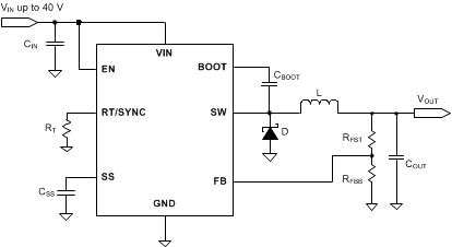
4 Simplified Schematic

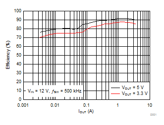
Efficiency vs Output Current
