SNVS441I January 2007 – November 2016 LP5521
PRODUCTION DATA.
- 1 Features
- 2 Applications
- 3 Description
- 4 Revision History
- 5 Pin Configuration and Functions
-
6 Specifications
- 6.1 Absolute Maximum Ratings
- 6.2 ESD Ratings
- 6.3 Recommended Operating Conditions
- 6.4 Thermal Information
- 6.5 Electrical Characteristics
- 6.6 Charge Pump Electrical Characteristics
- 6.7 LED Driver Electrical Characteristics (R, G, B Outputs)
- 6.8 Logic Interface Characteristics
- 6.9 I2C Timing Requirements (SDA, SCL)
- 6.10 Typical Characteristics
-
7 Detailed Description
- 7.1 Overview
- 7.2 Functional Block Diagram
- 7.3 Feature Description
- 7.4 Device Functional Modes
- 7.5 Programming
- 7.6
Register Maps
- 7.6.1 Enable Register (Enable)
- 7.6.2 Operation Mode Register (OP Mode)
- 7.6.3 R Channel PWM Control (R_PWM)
- 7.6.4 G Channel PWM Control (G_PWM)
- 7.6.5 B Channel PWM Control (B_PWM)
- 7.6.6 R Channel Current (R_CURRENT)
- 7.6.7 G Channel Current (G_CURRENT)
- 7.6.8 B Channel Current (B_CURRENT)
- 7.6.9 Configuration Control (CONFIG)
- 7.6.10 R Channel Program Counter Value (R Channel PC)
- 7.6.11 G Channel Program Counter Value (G Channel PC)
- 7.6.12 B Channel Program Counter Value (B Channel PC)
- 7.6.13 Status/Interrupt Register
- 7.6.14 RESET Register
- 7.6.15 GPO Register
- 7.6.16 Program Memory
- 8 Application and Implementation
- 9 Power Supply Recommendations
- 10Layout
- 11Device and Documentation Support
- 12Mechanical, Packaging, and Orderable Information
パッケージ・オプション
メカニカル・データ(パッケージ|ピン)
サーマルパッド・メカニカル・データ
発注情報
1 Features
- Adaptive Charge Pump With 1× and 1.5× Gain Provides Up to 95% LED Drive Efficiency
- Charge Pump with Soft Start and Overcurrent, Short-Circuit Protection
- Low Input Ripple and EMI
- Very Small Solution Size, No Inductor or Resistors Required
- 200-nA Typical Shutdown Current
- Automatic Power Save Mode
- I2C-Compatible Interface
- Independently Programmable Constant Current Outputs with 8-Bit Current Setting and 8-Bit PWM Control
- Typical LED Output Saturation Voltage 50 mV and Current Matching 1%
- Three Program Execution Engines with Flexible Instruction Set
- Autonomous Operation Without External Control
- Large SRAM Program Memory
- Two General Purpose Digital Outputs
2 Applications
- Fun and Indicator Lights
- LCD Sub-Display Backlighting
- Keypad RGB Backlighting and Phone Cosmetics
- Vibra, Speakers, Waveform Generator
- Blood Glucose Meter
- Handheld POS Terminals
- Electronic Access Control
- Where RGB Indication is Needed
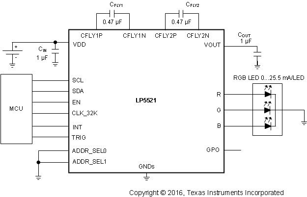
Typical Application Circuit

3 Description
The LP5521 is a three-channel LED driver designed to produce variety of lighting effects for mobile devices. A high-efficiency charge pump enables LED driving over full Li-Ion battery voltage range. The device has a program memory for creating variety of lighting sequences. When program memory has been loaded, LP5521 can operate autonomously without processor control allowing power savings.
The device maintains excellent efficiency over a wide operating range by automatically selecting proper charge pump gain based on LED forward voltage requirements and is able to automatically enter power-save mode, when LED outputs are not active and thus lowering current consumption.
Three independent LED channels have accurate programmable current sources and PWM control. Each channel has program memory for creating desired lighting sequences with PWM control.
The LP5521 has a flexible digital interface. Trigger I/O and a 32-kHz clock input allow synchronization between multiple devices. Interrupt output can be used to notify processor, when LED sequence has ended. The LP5521 has four pin selectable I2C-compatible addresses. This allows connecting up to four parallel devices in one I2C-compatible bus. GPO and INT pins can be used as a digital control pin for other devices.
The LP5521 requires only four small, low-cost ceramic capacitors.
Comprehensive application tools are available, including command compiler for easy LED sequence programming.
Device Information(1)
| PART NUMBER | PACKAGE | BODY SIZE |
|---|---|---|
| LP5521TM | DSBGA (20) | 2.093 mm × 1.733 mm (MAX) |
| LP5521YQ | WQFN (24) | 5.00 mm × 4.00 mm (NOM) |
- For all available packages, see the orderable addendum at the end of the data sheet.
4 Revision History
Changes from H Revision (May 2016) to I Revision
- Changed wording of title Go
Changes from G Revision (September 2014) to H Revision
- Added several new Applications Go
- Changed Body Size of DSBGA package to MAX dimensions Go
- Changed Handling Ratings to ESD Ratings table Go
- Changed RθJA value for DSBGA from 50 – 90°C/W to 70.7°C/W and WQFN from 37 – 90°C/W to 38.4°C/W; add additional thermal informationGo
- Added Community Resources Go
Changes from F Revision (February 2013) to G Revision
- Added Pin Configuration and Functions section, Handling Rating table, Feature Description section, Device Functional Modes, Application and Implementation section, Power Supply Recommendations section, Layout section, Device and Documentation Support section, and Mechanical, Packaging, and Orderable Information section Go