SBOS630D December 2013 – August 2016 OPA857
PRODUCTION DATA.
- 1 Features
- 2 Applications
- 3 Description
- 4 Revision History
- 5 Pin Configuration and Functions
- 6 Specifications
- 7 Detailed Description
- 8 Application and Implementation
- 9 Power-Supply Recommendations
- 10Layout
- 11Device and Documentation Support
- 12Mechanical, Packaging, and Orderable Information
パッケージ・オプション
メカニカル・データ(パッケージ|ピン)
- RGT|16
サーマルパッド・メカニカル・データ
- RGT|16
発注情報
1 Features
- Internal Midscale Reference Voltage
- Pseudo-Differential Output Voltage
- Wide Dynamic Range
- Closed-Loop Transimpedance Bandwidth:
- 125 MHz (5-kΩ Transimpedance Gain,
1.5-pF External Parasitic Capacitance) - 105 MHz (20-kΩ Transimpedance Gain,
1.5-pF External Parasitic Capacitance)
- 125 MHz (5-kΩ Transimpedance Gain,
- Ultralow Input-Referred Current Noise
(Brickwall Filter BW = 135 MHz):
15 nARMS (20-kΩ Transimpedance) - Very Fast Overload Recovery Time: < 25 ns
- Internal Input Protection Diode
- Power Supply:
- Extended Temperature Range: –40°C to +85°C
2 Applications
3 Description
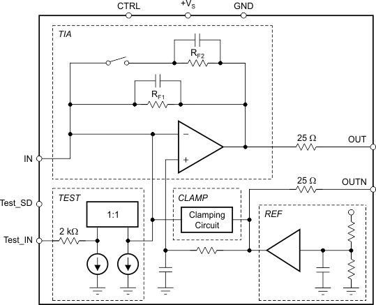
The OPA857 is a wideband, fast overdrive recovery, fast-settling, ultralow-noise transimpedance amplifier targeted at photodiode monitoring applications. With selectable feedback resistance, the OPA857 simplifies the design of high-performance optical systems. Very fast overload recovery time and internal input protection provide the best combination to protect the remainder of the signal chain from overdrive while minimizing recovery time. The two selectable transimpedance gain configurations allow high dynamic range and flexibility required in modern transimpedance amplifier applications. The OPA857 is available in a 3-mm × 3-mm VQFN package.
The device is characterized for operation over the full industrial temperature range from –40°C to +85°C.
Device Information(1)
| DEVICE NAME | PACKAGE | BODY SIZE |
|---|---|---|
| OPA857 | VQFN (16) | 3 mm × 3 mm |
- For all available packages, see the package option addendum at the end of the datasheet.
