SLOS814D March   2014  – September 2016 TAS5421-Q1

PRODUCTION DATA.  

  1. Features
  2. Applications
  3. Description
  4. Revision History
  5. Pin Configuration and Functions
  6. Specifications
    1. 6.1 Absolute Maximum Ratings
    2. 6.2 ESD Ratings
    3. 6.3 Recommended Operating Conditions
    4. 6.4 Thermal Information
    5. 6.5 Electrical Characteristics
    6. 6.6 Timing Requirements for I2C Interface Signals
    7. 6.7 Typical Characteristics
  7. Detailed Description
    1. 7.1 Overview
    2. 7.2 Functional Block Diagram
    3. 7.3 Feature Description
      1. 7.3.1 Analog Audio Input and Preamplifier
      2. 7.3.2 Pulse-Width Modulator (PWM)
      3. 7.3.3 Gate Drive
      4. 7.3.4 Power FETs
      5. 7.3.5 Load Diagnostics
      6. 7.3.6 Protection and Monitoring
      7. 7.3.7 I2C Serial Communication Bus
        1. 7.3.7.1 I2C Bus Protocol
        2. 7.3.7.2 Random Write
        3. 7.3.7.3 Random Read
        4. 7.3.7.4 Sequential Read
    4. 7.4 Device Functional Modes
      1. 7.4.1 Hardware Control Pins
      2. 7.4.2 EMI Considerations
      3. 7.4.3 Operating Modes and Faults
    5. 7.5 Register Maps
      1. 7.5.1 I2C Address Register Definitions
  8. Application and Implementation
    1. 8.1 Application Information
    2. 8.2 Typical Application
      1. 8.2.1 Design Requirements
        1. 8.2.1.1 Amplifier Output Filtering
        2. 8.2.1.2 Amplifier Output Snubbers
        3. 8.2.1.3 Bootstrap Capacitors
        4. 8.2.1.4 Analog Audio Input Filter
      2. 8.2.2 Detailed Design Procedure
        1. 8.2.2.1 Unused Pin Connections
          1. 8.2.2.1.1 MUTE Pin
          2. 8.2.2.1.2 STANDBY Pin
          3. 8.2.2.1.3 I2C Pins (SDA and SCL)
          4. 8.2.2.1.4 Terminating Unused Outputs
          5. 8.2.2.1.5 Using a Single-Ended Audio Input
      3. 8.2.3 Application Curves
  9. Power Supply Recommendations
  10. 10Layout
    1. 10.1 Layout Guidelines
    2. 10.2 Layout Examples
      1. 10.2.1 Top Layer
      2. 10.2.2 Second Layer - Signal Layer
      3. 10.2.3 Third Layer - Power Layer
      4. 10.2.4 Bottom Layer - Ground Layer
  11. 11Device and Documentation Support
    1. 11.1 Device Support
      1. 11.1.1 Third-Party Products Disclaimer
    2. 11.2 Documentation Support
      1. 11.2.1 Related Documentation
    3. 11.3 Receiving Notification of Documentation Updates
    4. 11.4 Community Resource
    5. 11.5 Trademarks
    6. 11.6 Electrostatic Discharge Caution
    7. 11.7 Glossary
  12. 12Mechanical, Packaging, and Orderable Information

パッケージ・オプション

メカニカル・データ(パッケージ|ピン)
サーマルパッド・メカニカル・データ
発注情報

1 Features

  • Mono BTL Digital Power Amplifier
  • 22-W Output Power at 10% THD+N into 4 Ω
  • 4.5-V to 18-V Operating Range
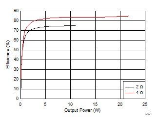
  • 85% Efficiency into 4 Ω
  • Differential Analog Input
  • Speaker Guard™ Speaker Protection with Adjustable Power Limiter
  • 75-dB Power-Supply Rejection Ratio (PSRR)
  • Load Diagnostic Functions:
    • Open and Shorted Output Load
    • Output-to-Power and Output-to-Ground Shorts
  • Protection and Monitoring Functions:
    • Short-Circuit Protection
    • 40-V Load Dump Protection per ISO-7637-2
    • Output DC Level Detection while Music is Playing
    • Overtemperature Protection
    • Overvoltage and Undervoltage Protection
  • Thermally Enhanced 16-Pin HTSSOP (PWP) Package with PowerPAD™ Package (Pad Down)
  • Designed for Automotive EMC Requirements
  • Qualified According to AEC-Q100 Grade 2
  • ISO9000: 2002 TS16949 Certified
  • –40°C to 125°C Ambient Temperature Range

2 Applications

  • Automotive Emergency Call (eCall) Amplifier
  • Telematics Systems
  • Instrument Cluster Systems
  • Infotainment Audio

3 Description

The TAS5421-Q1 is a mono digital audio amplifier, ideal for use in automotive emergency call (eCall), telematics, instrument cluster, and infotainment applications. The device provides up to 22 W into 4 Ω at less than 10% THD+N from a 14.4-Vdc automotive battery. The wide operating voltage range and excellent efficiency make the device ideal for start-stop support or running from a backup battery when required. The integrated load-dump protection reduces external voltage clamp cost and size, and the onboard load diagnostics report the status of the speaker through I2C.

Device Information(1)

PART NUMBER PACKAGE BODY SIZE (NOM)
TAS5421-Q1 HTSSOP (16) 5.00 mm × 4.40 mm
  1. For all available packages, see the orderable addendum at the end of the datasheet.


Simplified Block Diagram

TAS5421-Q1 sim-sch_SLOS814.gif

Output Power Efficiency

TAS5421-Q1 D001_SLOS814.gif