SLAS784A March 2012 – September 2015 TLV320AIC3212
PRODUCTION DATA.
- 1 Features
- 2 Applications
- 3 Description
- 4 Revision History
- 5 Description (continued)
- 6 Device Comparison Table
- 7 Pin Configuration and Functions
-
8 Specifications
- 8.1 Absolute Maximum Ratings
- 8.2 ESD Ratings
- 8.3 Recommended Operating Conditions
- 8.4 Thermal Information
- 8.5 Electrical Characteristics, SAR ADC
- 8.6 Electrical Characteristics, ADC
- 8.7 Electrical Characteristics, Bypass Outputs
- 8.8 Electrical Characteristics, Microphone Interface
- 8.9 Electrical Characteristics, Audio DAC Outputs
- 8.10 Electrical Characteristics, Class-D Outputs
- 8.11 Electrical Characteristics, Miscellaneous
- 8.12 Electrical Characteristics, Logic Levels
- 8.13 Audio Data Serial Interface Timing (I2S): I2S/LJF/RJF Timing in Master Mode
- 8.14 Audio Data Serial Interface Timing (I2S): I2S/LJF/RJF Timing in Slave Mode
- 8.15 Typical DSP Timing: DSP/Mono PCM Timing in Master Mode
- 8.16 Typical DSP Timing: DSP/Mono PCM Timing in Slave Mode
- 8.17 I2C Interface Timing
- 8.18 SPI Timing
- 8.19 Typical Characteristics
- 9 Parameter Measurement Information
-
10Detailed Description
- 10.1 Overview
- 10.2 Functional Block Diagram
- 10.3
Feature Description
- 10.3.1 Device Connections
- 10.3.2
Analog Audio I/O
- 10.3.2.1 Analog Low Power Bypass
- 10.3.2.2
Headphone Outputs
- 10.3.2.2.1 Using the Headphone Amplifier
- 10.3.2.2.2 Ground-Centered Headphone Amplifier Configuration
- 10.3.2.2.3 Stereo Unipolar Configuration
- 10.3.2.2.4 Mono Differential DAC to Mono Differential Headphone Output
- 10.3.2.3 Stereo Line Outputs
- 10.3.2.4 Differential Receiver Output
- 10.3.2.5 Stereo Class-D Speaker Outputs
- 10.3.3 ADC / Digital Microphone Interface
- 10.3.4 DAC
- 10.3.5 Device Power Consumption
- 10.3.6 Powertune
- 10.3.7 Clock Generation and PLL
- 10.3.8 Interfaces
- 10.3.9 Device Special Functions
- 10.4 Device Functional Modes
- 10.5 Register Maps
- 11Application and Implementation
- 12Power Supply Recommendations
- 13Layout
- 14Device and Documentation Support
- 15Mechanical, Packaging, and Orderable Information
1 Features
- Stereo Audio DAC With 101=dB SNR
- 2.7-mW Stereo 48-kHz DAC Playback
- Stereo Audio ADC With 93-dB SNR
- 5.6-mW Stereo 48-kHz ADC Record
- 8 kHz to 192 kHz Playback and Record
- 30-mW DirectPath™ Headphone Driver Eliminates Large Output DC-Blocking Capacitors
- 128-mW Differential Receiver Output Driver
- Stereo Class-D Speaker Drivers
- 1.7 W (8 Ω, 5.5 V, 10% THDN)
- 1.4 W (8 Ω, 5.5 V, 1% THDN)
- Stereo Line Outputs
- PowerTune™ - Adjusts Power vs SNR
- Extensive Signal Processing Options
- Eight Single-Ended or 4 Fully-Differential Analog Inputs
- Stereo Digital and Analog Microphone Inputs
- Low Power Analog Bypass Mode
- Programmable PLL, Plus Low-Frequency Clocking
- Programmable 12-Bit SAR ADC
- SPI and I2C Control Interfaces
- Three Independent Digital Audio Serial Interfaces
- 4.81 mm × 4.81 mm × 0.625 mm 81-Ball WCSP (YZF) Package
2 Applications
- Mobile Handsets
- Tablets and eBooks
- Portable Navigation Devices (PND)
- Portable Media Players (PMP)
- Portable Gaming Systems
- Portable Computing
3 Description
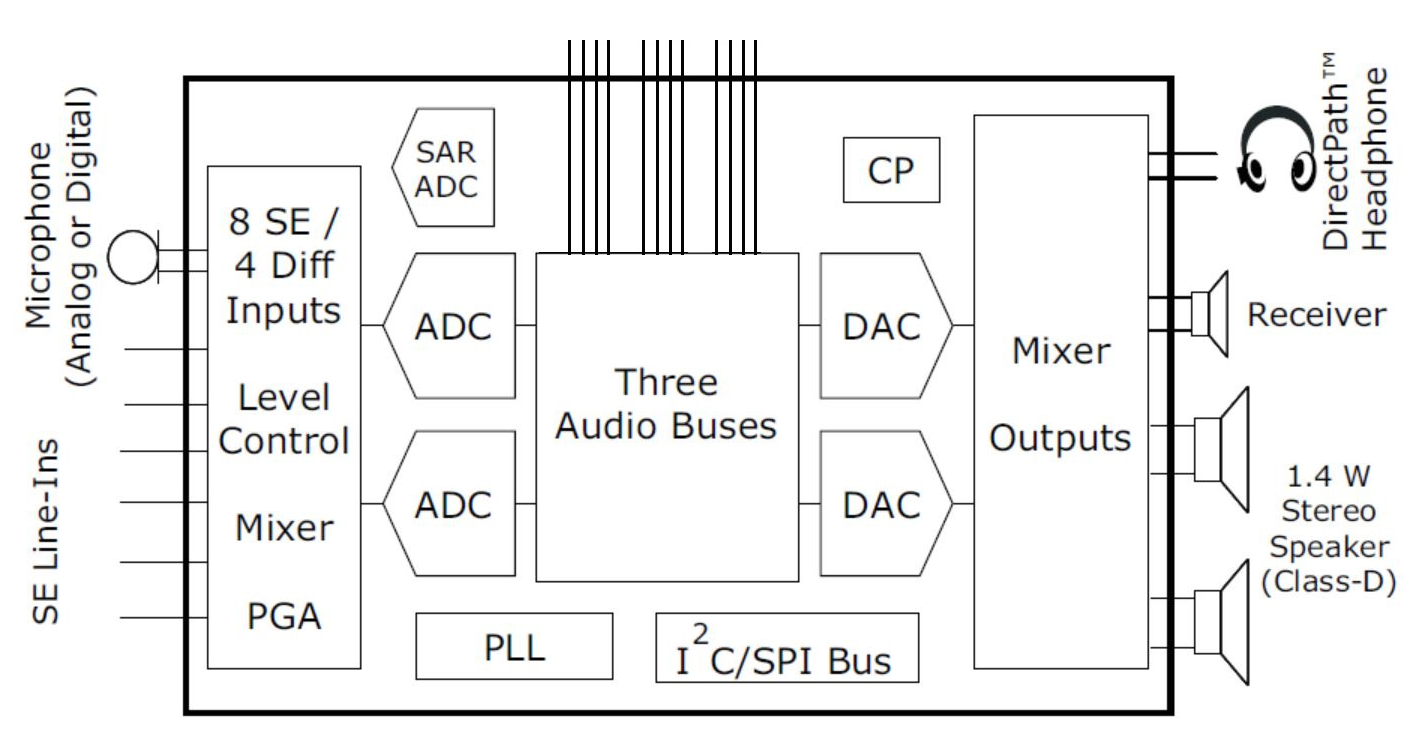
The TLV320AIC3212 (also referred to as the AIC3212) device is a flexible, highly-integrated, low-power, low-voltage stereo audio codec. The AIC3212 features digital microphone inputs and programmable outputs, PowerTune capabilities, selectable audio-processing blocks, predefined and parameterizable signal processing blocks, integrated PLL, and flexible audio interfaces. Extensive register-based control of power, input and output channel configuration, gains, effects, pin-multiplexing and clocks are included, allowing the device to be precisely targeted to its application.
Device Information(1)
| PART NUMBER | PACKAGE | BODY SIZE (NOM) |
|---|---|---|
| TLV320AIC3212 | DSBGA (81) | 4.81 mm × 4.81 mm |
- For all available packages, see the orderable addendum at the end of the data sheet.
Simplified Block Diagram
