SLVS279D March 2000 – August 2015 TPS61000 , TPS61002 , TPS61005 , TPS61006 , TPS61007
PRODUCTION DATA.
- 1 Features
- 2 Applications
- 3 Description
- 4 Revision History
- 5 Available Options
- 6 Pin Configuration and Functions
- 7 Specifications
- 8 Parameter Measurement Information
- 9 Detailed Description
- 10Application and Implementation
- 11Power Supply Recommendations
- 12Layout
- 13Device and Documentation Support
- 14Mechanical, Packaging, and Orderable Information
デバイスごとのパッケージ図は、PDF版データシートをご参照ください。
メカニカル・データ(パッケージ|ピン)
- DGS|10
サーマルパッド・メカニカル・データ
1 Features
- Start-Up Into a Full Load With Supply Voltages as Low as 0.9 V Over Full Temperature Range
- Minimum 100-mA Output Current From 0.8-V Supply Voltage, 250 mA From 1.8 V
- High Power Conversion Efficiency, up to 90%
- Power-Save Mode for Improved Efficiency at Low Output Currents
- Device Quiescent Current Less Than 50 µA
- Added System Security With Integrated Low-Battery Comparator
- Low-EMI Converter (Integrated Antiringing Switch Across Inductor)
- Micro-Size 10-Pin MSOP Package
- Evaluation Modules Available (TPS6100xEVM–156)
2 Applications
- Single- and Dual-Cell Battery Operated Products
- MP3-Players and Wireless Headsets
- Pagers and Cordless Phones
- Portable Medical Diagnostic Equipment
- Remote Controls
3 Description
The TPS6100x devices are boost converters intended for systems that are typically operated from a single- or dual-cell nickel-cadmium (NiCd), nickel-metal hydride (NiMH), or alkaline battery. The converter output voltage can be adjusted from 1.5 V to a maximum of 3.3 V and provides a minimum output current of 100 mA from a single battery cell and 250 mA from two battery cells. The converter starts up into a full load with a supply voltage of 0.9 V and stays in operation with supply voltages as low as 0.8 V.
The converter is based on a fixed-frequency, current-mode pulse-width-modulation (PWM) controller that goes into power-save mode at low load currents. The current through the switch is limited to a maximum of 1100 mA, depending on the output voltage. The current sense is integrated to further minimize external component count. The converter can be disabled to minimize battery drain when the system is put into standby.
A low-EMI mode is implemented to reduce interference and radiated electromagnetic energy that is caused by the ringing of the inductor when the inductor discharge-current decreases to zero. The device is packaged in the space-saving 10-pin MSOP package.
Device Information(1)
| PART NUMBER | PACKAGE | BODY SIZE (NOM) |
|---|---|---|
| TPS6100x | VSSOP (10) | 3.00 mm × 3.00 mm |
- For all available packages, see the orderable addendum at the end of the datasheet.
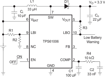
Typical Application Circuit for Fixed Output Voltage Options

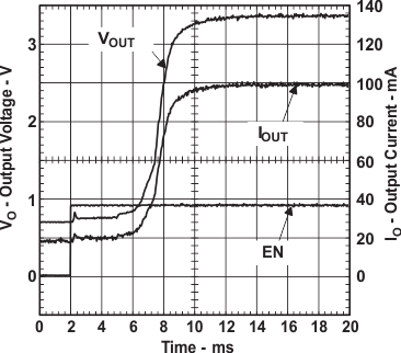
TPS61006 Start-Up Timing Into 33-Ω Load
