SLVSAE3A August 2010 – January 2016 TPS650231
PRODUCTION DATA.
- 1 Features
- 2 Applications
- 3 Description
- 4 Revision History
- 5 Description (continued)
- 6 Pin Configuration and Functions
-
7 Specifications
- 7.1 Absolute Maximum Ratings
- 7.2 ESD Ratings
- 7.3 Recommended Operating Conditions
- 7.4 Thermal Information
- 7.5 Electrical Characteristics
- 7.6 Electrical Characteristics: Control Signals
- 7.7 Electrical Characteristics: Supply Pins VCC, VINDCDC1, VINDCDC2, VINDCDC3, VINDCDC13
- 7.8 Electrical Characteristics: Supply Pins VBACKUP, VSYSIN, VRTC, VINLDO
- 7.9 Electrical Characteristics: VDCDC1 Step-Down Converter
- 7.10 Electrical Characteristics: VDCDC2 Step-Down Converter
- 7.11 Electrical Characteristics: VDCDC3 Step-Down Converter
- 7.12 Timing Requirements
- 7.13 Typical Characteristics
-
8 Detailed Description
- 8.1 Overview
- 8.2 Functional Block Diagrams
- 8.3
Feature Description
- 8.3.1 VRTC Output and Operation With or Without Backup Battery
- 8.3.2 Step-Down Converters, VDCDC1, VDCDC2, and VDCDC3
- 8.3.3 Power Save Mode Operation
- 8.3.4 Low-Ripple Mode
- 8.3.5 Soft-Start
- 8.3.6 100% Duty Cycle Low-Dropout Operation
- 8.3.7 Active Discharge When Disabled
- 8.3.8 Power-Good Monitoring
- 8.3.9 Low-Dropout Voltage Regulators
- 8.3.10 Undervoltage Lockout
- 8.3.11 Power-Up Sequencing
- 8.3.12 System Reset + Control Signals
- 8.4 Device Functional Modes
- 8.5 Programming
- 8.6
Register Maps
- 8.6.1 VERSION Register Address: 00h (Read Only)
- 8.6.2 PGOODZ Register Address: 01h (Read Only)
- 8.6.3 MASK Register Address: 02h (Read or Write), Default Value: C0h
- 8.6.4 REG_CTRL Register Address: 03h (Read or Write), Default Value: FFh
- 8.6.5 CON_CTRL Register Address: 04h (Read or Write), Default Value: B1h
- 8.6.6 CON_CTRL2 Register Address: 05h (Read or Write), Default Value: 40h
- 8.6.7 DEFCORE Register Address: 06h (Read or Write), Default Value: 14h/1Eh
- 8.6.8 DEFSLEW Register Address: 07h (Read or Write), Default Value: 06h
- 8.6.9 LDO_CTRL Register Address: 08h (Read or Write), Default Value: Set with DEFLDO1 and DEFLDO2
- 9 Application and Implementation
- 10Power Supply Recommendations
- 11Layout
- 12Device and Documentation Support
- 13Mechanical, Packaging, and Orderable Information
パッケージ・オプション
メカニカル・データ(パッケージ|ピン)
サーマルパッド・メカニカル・データ
- RSB|40
発注情報
1 Features
- 1.7-A, 90% Efficient Step-Down Converter for Processor Core (VDCDC1)
- 1.2-A, Up to 95% Efficient Step-Down Converter for System Voltage (VDCDC2)
- 0.8-A, 92% Efficient Step-Down Converter for Memory Voltage (VDCDC3)
- 30-mA LDO and Switch for Real-Time Clock (VRTC)
- 2 × 200-mA General-Purpose LDO
- Dynamic Voltage Management for Processor Core
- Preselectable LDO Voltage Using Two Digital Input Pins
- Externally Adjustable Reset Delay Time
- Battery Backup Functionality
- Separate Enable Pins for Inductive Converters
- I2C™-Compatible Serial Interface
- 85-μA Quiescent Current
- Low-Ripple PFM Mode
- Thermal Shutdown Protection
- Available in 40-Pin, 5-mm × 5-mm VQFN (RSB) or 49-Ball, 3-mm × 3-mm DSBGA (YFF) Package
2 Applications
- Smart Phones
- Netbooks and MIDs
- Portable Media Players
3 Description
The TPS650231 device is an integrated power management IC for applications powered by one
Li-Ion or Li-Polymer cell, and which requires multiple power rails. The TPS650231 provides three highly efficient step-down converters targeted at providing the core voltage, peripheral, I/O, and memory rails in a processor-based system. The core converter allows for on-the-fly voltage changes through serial interface, allowing the system to implement dynamic power savings.
Device Information(1)
| PART NUMBER | PACKAGE | BODY SIZE (NOM) |
|---|---|---|
| TPS650231 | VQFN (40) | 5.00 mm × 5.00 mm |
| DSBGA (49) | 3.00 mm × 3.00 mm |
- For all available packages, see the orderable addendum at the end of the data sheet.
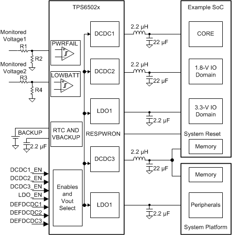
Simplified Schematic
