SLVSBK1E September   2012  – May 2014 TPS65631

PRODUCTION DATA.  

  1. Features
  2. Applications
  3. Description
  4. Simplified Schematic
  5. Revision History
  6. Pin Configuration and Functions
  7. Specifications
    1. 7.1 Absolute Maximum Ratings
    2. 7.2 Handling Ratings
    3. 7.3 Recommended Operating Conditions
    4. 7.4 Thermal Information
    5. 7.5 Electrical Characteristics
    6. 7.6 Timing Requirements
    7. 7.7 Typical Characteristics
  8. Detailed Description
    1. 8.1 Overview
    2. 8.2 Functional Block Diagram
    3. 8.3 Feature Description
      1. 8.3.1 Boost Converter
      2. 8.3.2 Inverting Buck-Boost Converter
        1. 8.3.2.1 Programming VNEG
        2. 8.3.2.2 Controlling the VNEG Transition Time
      3. 8.3.3 Soft-Start and Start-Up Sequence
      4. 8.3.4 Enable (CTRL)
      5. 8.3.5 Undervoltage Lockout
      6. 8.3.6 Short Circuit Protection
        1. 8.3.6.1 Short-Circuits During Normal Operation
        2. 8.3.6.2 Short-Circuits During Start-Up
      7. 8.3.7 Output Discharge During Shutdown
      8. 8.3.8 Thermal Shutdown
    4. 8.4 Device Functional Modes
      1. 8.4.1 Operation with VI < 2.9 V
      2. 8.4.2 Operation with VI ≈ VPOS (Diode Mode)
      3. 8.4.3 Operation with CTRL
  9. Applications and Implementation
    1. 9.1 Application Information
    2. 9.2 Typical Application
      1. 9.2.1 Design Requirements
      2. 9.2.2 Detailed Design Procedure
        1. 9.2.2.1 Inductor Selection
        2. 9.2.2.2 Capacitor Selection
        3. 9.2.2.3 Stability
      3. 9.2.3 Application Curves
  10. 10Power Supply Recommendations
  11. 11Layout
    1. 11.1 Layout Guidelines
    2. 11.2 Layout Example
  12. 12Device and Documentation Support
    1. 12.1 Device Support
      1. 12.1.1 Third-Party Products Disclaimer
    2. 12.2 Trademarks
    3. 12.3 Electrostatic Discharge Caution
    4. 12.4 Glossary
  13. 13Mechanical, Packaging, and Orderable Information

パッケージ・オプション

メカニカル・データ(パッケージ|ピン)
サーマルパッド・メカニカル・データ
発注情報

1 Features

  • 2.9-V to 4.5-V Input Voltage Range
  • Fixed 4.6-V Positive Output Voltage
  • 0.5% VPOS Accuracy from 25ºC to 85ºC
  • Separate VPOS Output Sense Pin
  • Negative Output Voltage Digitally Programmable from –1.4 V to –4.4 V (–4 V Default)
  • Output Currents up to 250 mA Supported
  • Excellent Line Transient Regulation
  • Short-Circuit Protection
  • Thermal Shutdown
  • Available in 3.00-mm × 3.00-mm, 12-Pin QFN Package

2 Applications

    AMOLED Displays

3 Description

The TPS65631 is designed to drive AMOLED (Active Matrix Organic Light Emitting Diode) displays requiring positive and negative supply rails. The device integrates a boost converter for VPOS and an inverting buck boost converter for VNEG and is suitable for battery-operated products. The digital control pin (CTRL) allows programming the negative output voltage in digital steps. The TPS65631 uses a novel technology enabling excellent line transient performance.

Device Information(1)

PART NUMBER PACKAGE BODY SIZE (NOM)
TPS65631 QFN (12) 3.00 mm × 3.00 mm
  1. For all available packages, see the orderable addendum at the end of the data sheet
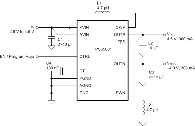
4 Simplified Schematic

Schem_01_SLVSBK1.gif

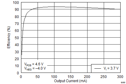
Efficiency vs Output Current

AppPerf_00_SLVSBK1.png