SBVS278A February 2016 – October 2016 TPS720-Q1
PRODUCTION DATA.
- 1 Features
- 2 Applications
- 3 Description
- 4 Revision History
- 5 Pin Configuration and Functions
- 6 Specifications
- 7 Detailed Description
- 8 Application and Implementation
- 9 Power Supply Recommendations
- 10Layout
- 11Device and Documentation Support
- 12Mechanical, Packaging, and Orderable Information
パッケージ・オプション
メカニカル・データ(パッケージ|ピン)
- DRV|6
サーマルパッド・メカニカル・データ
- DRV|6
発注情報
1 Features
- Qualified for Automotive Applications
- AEC-Q100 Qualified With the Following Results:
- Device Temperature Grade 1: –40°C to +125°C Ambient Operating Temperature Range
- Device HBM ESD Classification Level H2
- Device CDM ESD Classification Level C6
- Input Voltage Range: 1.1 V to 4.5 V
- Output Voltage Range: 0.9 V to 3.6 V
- High-Performance LDO: 350 mA
- Low Quiescent Current: 38 μA
- Excellent Load Transient Response:
±15 mV for ILOAD = 0 mA to 350 mA in 1 μs - Low Noise: 48 μVRMS (10 Hz to 100 kHz)
- 80-dB VIN PSRR (10 Hz to 10 kHz)
- 70-dB VBIAS PSRR (10 Hz to 10 kHz)
- Fast Start-Up Time: 140 μs
- Built-In Soft-Start With Monotonic VOUT Rise and Start-Up Current Limited to 100 mA + ILOAD
- Overcurrent and Thermal Protection
- Low Dropout: 110 mV at ILOAD = 350 mA
- Stable With a 2.2-μF Output Capacitor
- Package: 2.00 mm × 2.00 mm, 6-Pin WSON
2 Applications
- Camera Modules
- FPD Link Power
- Automotive Infotainment
- USB HUB Power
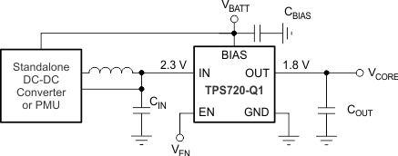
Simplified Schematic

3 Description
The TPS720-Q1 family of dual-rail, low-dropout linear regulators (LDOs) offers outstanding ac performance (PSRR, load and line transient response) and consume a very low quiescent current of 38 μA.
The VBIAS rail that powers the control circuit of the LDO draws very low current (on the order of the LDO quiescent current) and can be connected to any power supply that is equal to or greater than 1.4 V above the output voltage. The main power path is through VIN and can be a lower voltage than VBIAS; this path can be as low as VOUT + VDO, increasing the efficiency of the solution in many power-sensitive applications. For example, VIN can be an output of a high-efficiency, dc-dc, step-down regulator.
The TPS720-Q1 supports a novel feature where the output of the LDO regulates under light loads when the IN pin is left floating. The light-load drive current is sourced from VBIAS under this condition. This feature is particularly useful in power-saving applications where the dc-dc converter connected to the IN pin is disabled but the LDO is still required to regulate the voltage to a light load.
The TPS720-Q1 is stable with ceramic capacitors and uses an advanced BICMOS fabrication process that yields a dropout of 110 mV at a 350-mA output load. The TPS720-Q1 provides a monotonic VOUT rise (overshoot limited to 3%) with VIN inrush current limited to 100 mA + ILOAD with an output capacitor of 2.2 μF.
The TPS720-Q1 uses a precision voltage reference and feedback loop to achieve overall accuracy of 2% over load, line, process, and temperature extremes. The TPS720-Q1 is available in a 6-pin WSON package. This family of devices is fully specified over the temperature range of TJ = –40°C to +125°C.
Device Information(1)
| PART NUMBER | PACKAGE | BODY SIZE (NOM) |
|---|---|---|
| TPS720-Q1 | WSON (6) | 2.00 mm × 2.00 mm |
- For all available packages, see the orderable addendum at the end of the data sheet.
4 Revision History
Changes from * Revision (February 2016) to A Revision
- Changed Output Voltage Range bullet in Features section from "0.9 V to 3.0 V" to "0.9 V to 3.6 V"Go
- Changed maximum value of "output voltage" parameter from 3.0 V to 3.6 V in Recommended Operating Conditions tableGo
- Reformatted Thermal Information table note Go
- Changed maximum value of output voltage parameter from 3.0 V to 3.6 V in Electrical Characteristics table Go
- Changed output voltage range in table note from "0.9 V to 3.0 V" to "0.9 V to 3.3 V" in Device Nomenclature sectionGo
- Changed formatting of Related Documentation section Go
- Added Receiving Notification of Documentation Updates section Go