SLVSCT1B February 2015 – April 2015 TPS92512 , TPS92512HV
PRODUCTION DATA.
- 1 Features
- 2 Applications
- 3 Description
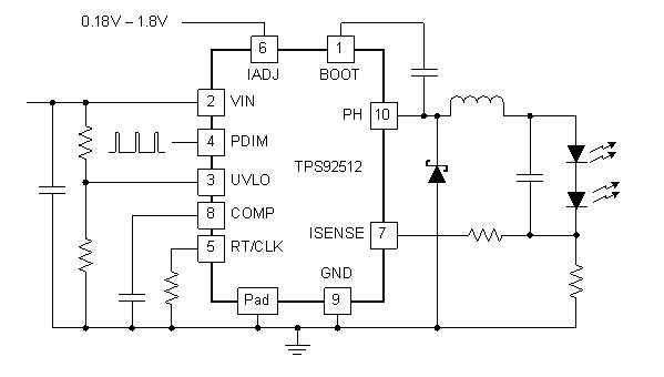
- 4 Simplified Schematics
- 5 Revision History
- 6 Pin Configuration and Functions
- 7 Specifications
-
8 Detailed Description
- 8.1 Overview
- 8.2 Functional Block Diagram
- 8.3
Feature Description
- 8.3.1 Undervoltage Lockout and Low Power Shutdown (UVLO Pin)
- 8.3.2 Adjustable Switching Frequency (RT/CLK Pin)
- 8.3.3 Synchronizing the Switching Frequency to an External Clock (RT/CLK Pin)
- 8.3.4 Adjustable LED Current (IADJ and ISENSE Pins)
- 8.3.5 PWM Dimming (PDIM Pin)
- 8.3.6 External Compensation (COMP Pin)
- 8.3.7 Overcurrent Protection
- 8.3.8 Overtemperature Protection
- 8.4 Device Functional Modes
-
9 Application and Implementation
- 9.1 Application Information
- 9.2 Typical Application
- 9.3 Design Requirements
- 9.4
Detailed Design Procedure
- 9.4.1 Standard Component Selection
- 9.4.2 Calculate UVLO Resistor Values
- 9.4.3 Calculate the RT Resistor Value (RRT)
- 9.4.4 Calculate the ISENSE Resistor Value (R(ISENSE))
- 9.4.5 Calculate the Inductor Value and Operating Parameters (L)
- 9.4.6 Calculate the Minimum Input Capacitance and the Required RMS Current Rating (CIN)
- 9.4.7 Calculate the Output Capacitor Value (COUT)
- 9.4.8 Calculate the Diode Power Dissipation (D)
- 9.5 Application Curves
- 10Power Supply Recommendations
- 11Layout
- 12Device and Documentation Support
- 13Mechanical, Packaging, and Orderable Information
パッケージ・オプション
メカニカル・データ(パッケージ|ピン)
- DGQ|10
サーマルパッド・メカニカル・データ
- DGQ|10
発注情報
1 Features
- Integrated 200-mΩ High-Side MOSFET
- 4.5-V to 42-V Input Voltage Range
(4.5 V to 60 V for the TPS92512HV) - 0 V to 300 mV Adjustable Voltage Reference
- ±5% LED Current Accuracy
- 100-kHz to 2-MHz Switching Frequency Range
- Dedicated PWM Dimming Input
- Adjustable Undervoltage-Lock-Out
- Overcurrent Protection
- Overtemperature Protection
- MSOP-10 Package with PowerPAD™
2 Applications
- Street Lighting
- Emergency/Exit Lighting
- General Industrial and Commercial Illumination
- Retail Lighting
- Appliance Lighting
- Transportation Lighting
- Channel Letters
- Light Bars
3 Description
The TPS92512/HV are 2.5A step-down (buck) current regulators with an integrated MOSFET to drive high current LEDs. Available with 42 V and 60 V (HV) input ranges, these LED drivers operate at a user selected fixed-frequency with peak-current mode control and deliver excellent line and load regulation.
The TPS92512/HV LED drivers feature separate inputs for analog and pulse width modulation (PWM) dimming for no compromise brightness control achieving contrast ratios of greater than 10:1 and greater than 100:1, respectively. The PWM input is compatible with low-voltage logic standards for easy interface to a broad range of microcontrollers. The analog LED current setpoint is adjustable from 0 V to 300 mV using the IADJ input with an external 0 V to 1.8 V signal.
For multi-string applications using two or more TPS92512/HV LED drivers, the internal oscillator can be overdriven by an external clock ensuring all of the converters operate at a common frequency thereby reducing the potential for beat frequencies and simplifying system EMI filtering. An adjustable input under-voltage lockout (UVLO) with hysteresis provides flexibility in setting start/stop voltages based upon supply voltage conditions.
The TPS92512 includes cycle-by-cycle overcurrent protection and thermal shutdown protection. It is available in a 10-pin HVSSOP PowerPAD™ package.
Device Information(1)
| PART NUMBER | PACKAGE | BODY SIZE (NOM) |
|---|---|---|
| TPS92512 | HVSSOP (10) | 5.00 mm x 3.00 mm |
| TPS92512HV |
- For all available packages, see the orderable addendum at the end of the data sheet.
4 Simplified Schematics

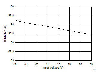
Efficiency vs Input Voltage
7 White LEDs at 1.5A (VOUT = 23 V)
