SBOT040C December 2020 – February 2022 OPA140 , OPA141 , OPA145 , OPA1641 , OPA1642 , OPA1644 , OPA182 , OPA189 , OPA191 , OPA192 , OPA196 , OPA197 , OPA2140 , OPA2141 , OPA2182 , OPA2189 , OPA2191 , OPA2192 , OPA2196 , OPA2197 , OPA2990 , OPA4140 , OPA4141 , OPA4182 , OPA4189 , OPA4191 , OPA4192 , OPA4196 , OPA4197 , OPA627 , OPA637 , OPA827 , OPA828 , TLV9102 , TLV9302
Application Brief
Introduction
Multiplexing is a technique that is frequently used to perform data acquisition in multichannel systems with minimal signal-chain requirements. In this context, the role of the multiplexer (MUX) in an acquisition system is to switch between channels, and send each signal to a single data converter as quickly as possible, thus maximizing system throughput and minimizing delay. To provide accurate processing, a precision amplifier is placed downstream from the multiplexer to precisely drive the analog-to-digital converter (ADC).
Traditional Amplifier Architecture
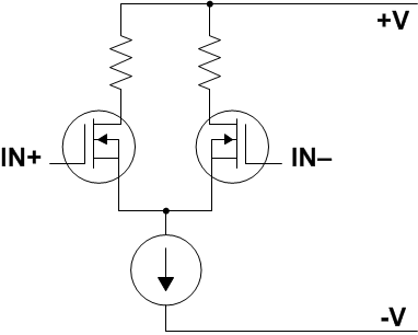
Traditional CMOS-input amplifier architectures consist of a differential transistor pair with the MOSFET sources connected together and then taken to ground via an active current source, as shown in Figure 1-1. Modern transistor manufacturing techniques attempt to maximize MOSFET transconductance (gm) by reducing oxide thickness (tox); however, this trade-off results in breakdown voltages of approximately 5 V from the gate to source. Large gate-to-source voltages typically stem from large input differential signals, which are commonly seen during slewing or open-loop operation. To protect the input from permanent damage, amplifiers have two robust anti-parallel diodes between the inputs of the amplifier with a clamp voltage of typically ±0.5 V to ±1.5 V. These diodes limit the voltage swing across the inputs to one or two forward-diode voltage drops, which is well below the breakdown voltage. While these inputs provide a level of protection, the inputs also have considerable drawbacks.
 Figure 1-1 Transistor Differential Input Pair
Large Differential Inputs With Traditional Op Amps
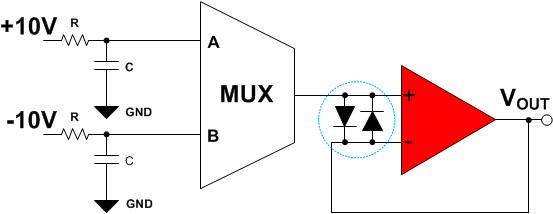
Figure 1-2 shows a MUX with two channels: A and B. When the output of the MUX is connected to channel A, 10 V is present at the non-inverting input of the op amp. The amplifier operates linearly; therefore, the potential across the inputs is 0 V (neglecting offset voltage). As soon as the MUX switches from channel A to channel B, the non-inverting input potential of the op amp instantly changes to –10 V. The op amp output voltage does not change instantly; a large differential voltage appears at the inputs, and the anti-parallel diodes begin to conduct current. This action causes a sharp increase in input bias current and drop in input impedance. Without the input anti-parallel diodes, this large differential voltage surpasses the breakdown voltage, and thus permanently damages the op amp. With the input anti-parallel diodes, outlined in blue in Figure 1-2, the inputs are protected from large differential voltages; however, large inrush current flows through the diodes. If passive filtering or high source impedance is present, large inrush current can disturb settling time, and thus limit system throughput and degrade signal-chain precision.
 Figure 1-2 MUX With Buffer-Configured Op Amp
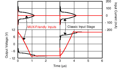
The op amp output settling time can be detrimental to high-speed or high-throughput applications. Most MUXes operate with nanosecond rise-times; far faster than most precision op amps. If the op amp slew rate cannot keep up with the MUX slew rate, a differential voltage develops, and settling time worsens as a result of input current. When the MUX switches between channels, an extended length of time is used for the output to respond to the input, and system performance may suffer. Some amplifiers attempt to solve this problem with high slew rate, but trade off power consumption and stability. TI’s Precision Amplifier team developed a unique patented technology that combines high slew rate with a diode-less front end to achieve accurate signal processing without the trade-offs of high-slew rate amplifiers. Device performance following a switched MUX is shown in Figure 1-3. Note the source-loading effects of a non-MUX-friendly amplifier (black) and a MUX-friendly amplifier (red). The top half of Figure 1-3 illustrates the inrush of current, which can reach several tens or hundreds of milliamperes depending on the amplifier output current limit. The bottom half of Figure 1-3 illustrates the effects of settling time while slewing. Although the traditional amplifier output moves quickly because of the input diodes, the RC-network settling is disturbed, and the system takes longer to settle.
 Figure 1-3 Switching Timing Diagram
MUX-Friendly Op Amps
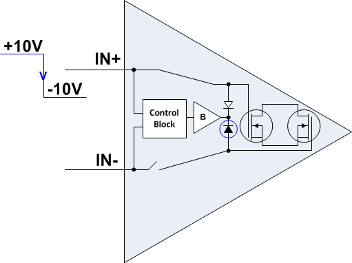
Along with JFET input amplifiers that are inherently MUX-friendly, TI developed a new input circuitry for 36-V CMOS inputs that does not require anti-parallel diodes for device protection. These MUX-friendly amplifiers maintain the same level of protection and robustness while improving settling time for switched systems. This patented input protection scheme uses a set of internal switches that open and close to protect the op amp input when large voltage steps are applied. This protection scheme has the added benefit of no inrush current. Figure 1-4 shows this new MUX-friendly protection scheme in the quiescent state, with both switches closed and the diodes inactive.
 Figure 1-4 MUX-Friendly Scheme
When the positive input goes low (+10 V to –10 V), the control block opens the switch at the inverting terminal (IN–) and activates one of the diodes, illustrated in Figure 1-5. When the positive input goes high (–10 V to + 10 V), the control block opens the switch at the non-inverting terminal (IN+) and activates the other diode.
 Figure 1-5 High-to-Low Input Step
The internal buffer op amp, labeled B, isolates the diode current from the input signal. The isolation prevents current from flowing through the input pins of the op amp. This new MUX-friendly architecture prevents any additional settling time. With this configuration, systems can quickly switch between MUX channels without compromising precision.
Additional Resources
| TI’s MUX-Friendly Op Amps | Recommended Multiplexers | |||||
|---|---|---|---|---|---|---|
| CMOS, Zero Drift, 36-V | CMOS, E-trim, 36-V | JFET-input, 36-V | CMOS, General Purpose, 40-V | General
Purpose, High Performance | High Voltage,
Low RON Flatness | Fault Protection |
|
0.02-μV/°C, 14-MHz 0.012-μV/˚C, 5-MHz 24-V, 750-kHz | 25-μV, 2.5-MHz 25-μV, 10-MHz Automotive | 150-μV, 5.5-MHz 120-μV, 11-MHz 300-μV, 45-MHz | 0.25-μV/°C, 10.6-MHz 0.6-μV/°C, 1.1-MHz 0.3-μV/°C, 4.5-MHz Automotive | 2:1x1 Channel, 36-V 2.1Ω RON 2:1x4 Channel, 44-V 3.5Ω RON 4:1x2 Channel, 44-V 3.5Ω RON Automotive | 1:1x4 Channel, 100-V 0.05Ω Flatness 4:1x2 Channel, 100-V 0.05Ω Flatness | 1:1x4 Channel, 44-V 60-V Overvoltage Protected 4:1x2 Channel, 44-V 60-V Overvoltage Protected |