SLVSDK1C May 2016 – September 2017 TPS22990
PRODUCTION DATA.
- 1 Features
- 2 Applications
- 3 Description
- 4 Revision History
- 5 Device Comparison Table
- 6 Pin Configuration and Functions
- 7 Specifications
- 8 Parameter Measurement Information
- 9 Detailed Description
- 10Application and Implementation
- 11Power Supply Recommendations
- 12Layout
- 13Device and Documentation Support
- 14Mechanical, Packaging, and Orderable Information
1 Features
- Integrated Single Channel Load Switch
- VBIAS Voltage Range: 2.5 V to 5.5 V
- VIN Voltage Range: 0.6 V to VBIAS
- On-Resistance
- RON = 3.9 mΩ (typical) at VIN = 5 V
(VBIAS = 5 V) - RON = 3.9 mΩ (typical) at VIN = 3.3 V
(VBIAS = 3.3 V)
- RON = 3.9 mΩ (typical) at VIN = 5 V
- 10-A Maximum Continuous Switch Current
- Quiescent Current
- IQ,VBIAS = 63 µA at VBIAS = 5 V
- Shutdown Current
- ISD,VBIAS = 5.5 µA at VBIAS = 5 V
- ISD,VIN = 4 nA at VBIAS = 5 V, VIN = 5 V
- Controlled and Adjustable Slew Rate through CT
- Power Good (PG) Indicator
- Quick Output Discharge (QOD) (TPS22990 Only)
- 3-mm × 2-mm SON 10-pin Package with Thermal Pad
- ESD Performance Tested per JESD 22
- 2-kV HBM and 1-kV CDM
2 Applications
- Notebooks, Chromebooks and Tablets
- Desktop PC and Industrial PC
- Solid State Drives (SSDs)
- Servers
- Telecom systems
3 Description
The TPS22990 product family consists of two devices: TPS22990 and TPS22990N. Each device is a 3.9-mΩ, single-channel load switch with a controlled and adjustable turn on and integrated PG indicator.
The devices contain an N-channel MOSFET that can operate over an input voltage range of 0.6 V to 5.5 V and can support a maximum continuous current of
10 A. The wide input voltage range and high current capability enable the devices to be used across multiple designs and end equipments. 3.9-mΩ On-resistance minimizes the voltage drop across the load switch and power loss from the load switch.
The controlled rise time for the device greatly reduces inrush current caused by large bulk load capacitances, thereby reducing or eliminating power supply droop. The adjustable slew rate through CT provides the design flexibility to trade off inrush current and power up timing requirements. Integrated PG indicator notifies the system about the status of the load switch to facilitate seamless power sequencing.
The TPS22990 has an optional 218-Ω On-chip resistor for quick discharge of the output when switch is disabled to avoid any unknown state caused by floating supply to the downstream load.
The TPS22990 is available in a small, space-saving
3-mm × 2-mm 10-SON package with integrated thermal pad allowing for high power dissipation. The device is characterized for operation over the free-air temperature range of –40°C to +105°C.
Device Information(1)
| PART NUMBER | PACKAGE | BODY SIZE (NOM) |
|---|---|---|
| TPS22990 TPS22990N |
WSON (10) | 3.00 mm × 2.00 mm |
- For all available packages, see the orderable addendum at the end of the data sheet.
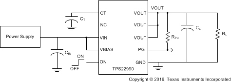
Typical Application

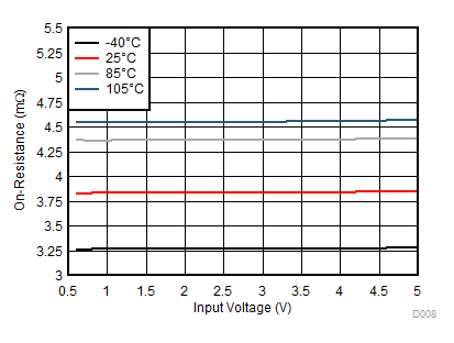
On-Resistance vs Input Voltage
